Flat panel display

a flat panel display and display panel technology, applied in the field of flat panel display, can solve the problems of deteriorating picture quality affecting the display effect, etc., and achieve the effect of different hues, without signal delay or voltage drop

Active Publication Date: 2006-05-11
SAMSUNG DISPLAY CO LTD
View PDF7 Cites 170 Cited by
  • Summary
  • Abstract
  • Description
  • Claims
  • Application Information

AI Technical Summary

Benefits of technology

[0009] The present invention addresses the issues associated with the conventional devices by providing a flat panel displ

Problems solved by technology

The zigzag path increases the resistance of the data line 1 and may delay a data signal.
The delay of the data signal along the data line 1 and the voltage drop along the power line 2 may deteriorate picture quality, which

Method used


Image

  • Flat panel display
  • Flat panel display
  • Flat panel display

Examples


first embodiment

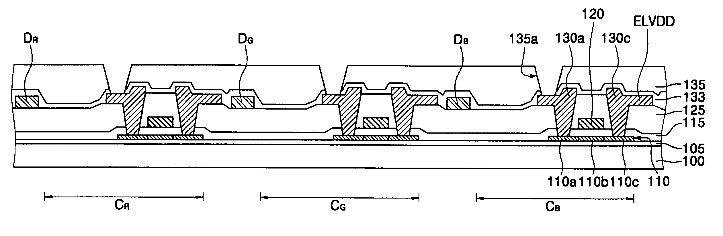
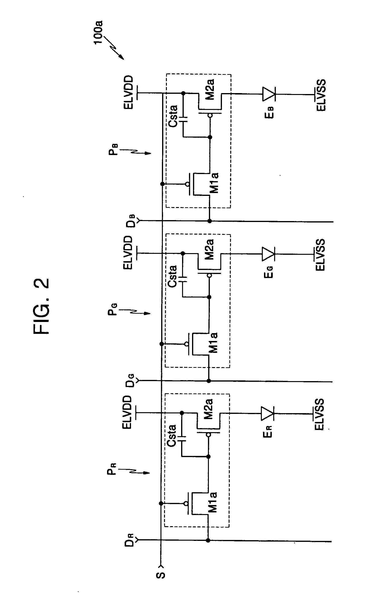
[0021]FIG. 2 is a circuit diagram of pixel driving circuits 100a in an OLED according to the present invention. Each of the pixel driving circuits 100a is coupled to signal lines, including a scan line S, a data line DR, DG, DB, and a power line ELVDD. The data lines DR, DG, DB include a red data line DR, a green data line DG, and a blue data line DB. The red, green, and blue data lines DR, DG, DB intersect the scan line S, thereby defining a red pixel PR, a green pixel PG, and a blue pixel PB. The red, green, and blue data lines DR, DG, DB are coupled to the red, green, and blue pixels PR, PG, PB, respectively. Therefore, a data signal having a certain color (red, green, or blue) is transmitted to a data line DR, DG, DB corresponding to the same color. This pixel driving circuit 100a is driven more easily than a circuit where the data signals corresponding to different colors are transmitted by the same data line.

[0022] The pixels include red, green, and blue light emitting diodes ...

second embodiment

[0042]FIG. 5 is a circuit diagram of a pixel driving circuit 100b in an OLED according to the present invention. An (n−1)th scan line S(n−1), an nth scan line S(n), a data line D, a power line ELVDD, and a pre-charge line Vint are coupled to the pixel driving circuit 100b. A pixel P is defined by intersection of the data line D and the scan line S(n). The pixel P includes a light emitting diode E and a pixel driving circuit 100b for driving the light emitting diode E that could be any of the red, green, or blue light emitting diodes ER, EG, EB. Depending on the light emitting diode ER, EG, EB, and the data line D, that could be a red, green, or blue data line DR, DG, DB, the pixel P may be a red, green, or blue pixel PR, PG, PB. The pixel driving circuit is composed of first through fourth transistors M1b, M2b, M3b, M4b, and a capacitor Cstb.

[0043] The first transistor M1b includes a gate coupled to the scan line S(n), and a source coupled to the data line D. The third transistor M3...

third embodiment

[0045]FIG. 6 is a circuit diagram of a pixel driving circuit 100c in an OLED according to the present invention. Signal lines, including a scan line S(n), a data line D, a power line ELVDD, and an emission control line EM(n) to the pixel driving circuit 100c. The data line D and the scan line S(n) intersect each other, defining a pixel P. The pixel P includes a light emitting diode E, that may be any of the red, green, or blue light emitting diodes ER, EG, EB, and a pixel driving circuit 100c for driving the light emitting diode E. The pixel driving circuit 100c includes first through third transistors M1c, M2c, M3c and a capacitor Cstc.

[0046] The first transistor M1c includes a gate coupled to the scan line S, and a source coupled to the data line D. The second transistor M2c includes a gate coupled to a drain of the first transistor M1c, and a source coupled to the power line ELVDD. The capacitor Cstc is coupled between the gate of the second transistor M2c and the power line ELVD...


PUM


Abstract

A flat panel display with good color mixture of three primary colors to achieve different hues and little signal delay is provided. The display includes signal lines including scan lines and data lines intersecting the scan lines, both arranged along straight lines. Red, green, and blue pixel driving circuit regions are defined by the intersection of the scan lines and the data lines. The pixel driving circuit regions having the same color are arranged adjacent to one another along a column direction. Red, green, and blue pixel driving circuits are placed in the pixel driving circuit regions and are coupled to the red, green, and blue pixel electrodes. The pixel electrodes are adjacent to pixel electrodes of a different color along both row and column directions.

Description

CROSS-REFERENCE TO RELATED APPLICATION [0001] This application claims priority to and the benefit of Korea Patent Application No. 2004-0090603, filed on Nov. 8, 2004, the entire content of which is incorporated herein by reference. BACKGROUND OF THE INVENTION [0002] 1. Field of the Invention [0003] The present invention relates to a flat panel display, and more particularly, to a full color flat panel display. [0004] 2. Description of the Related Art [0005] Flat panel displays are noted as substitutes for cathode ray tube displays because of their light weight, thin structure, and better image quality. Examples of the flat panel display include liquid crystal displays (LCD) and organic light emitting displays (OLED). As compared with the LCD, the OLED has superior brightness and viewing angle and does not require a backlight, which gives the OLED an advantage in realizing a thin display. [0006] Flat panel displays include red, green, and blue pixels for realizing a full color displa...

Claims


Application Information

Patent Timeline
IPC IPC(8): H01L51/00H05B44/00
CPCG09G3/3233G09G2300/0452G09G2300/0819G09G2300/0842G09G2300/0861G09G2320/0223G09G2320/0233H01L27/3211H01L27/3276H01L2251/5315H10K59/35H10K59/131H10K2102/3026G09G3/30
Inventor SUH, MI-SOOKKANG, TAE-WOOKLEE, UL-HO
Owner SAMSUNG DISPLAY CO LTD
Why Eureka
Try Eureka