Analog-to-digital converter operable with staggered timing

Inactive Publication Date: 2006-05-11
INFINEON TECH AG
View PDF11 Cites 41 Cited by
  • Summary
  • Abstract
  • Description
  • Claims
  • Application Information

AI Technical Summary

Benefits of technology

[0028] One advantage of the present invention may also be that a very low level of circuit complexity is necessary to reduce the incorrect adaptation in the output spectrum. In particular, the circuit complexity which results for the reduction of the incorrect adaptation is restricted to a connection network which can be configured at least once in order to implement the respective optimum converter sequence. In particular even when there is an increasing number of parallel individual analog-to-digital converters, the additional cost is low. All that is necessary here is a small amount of additional expenditure on sorting the individual analog-to-digital converters.
[0029] In this way the present invention is independent of the absolute precision of an identification algorithm such as is performed in known approaches to solutions which are acknowledged at the beginning. Although the present invention, accepts a certain degree of incorrect adaptation, the expenditure on circuitry and the computational complexity for reducing the incorrect adaptation is reduced greatly compared to previous approaches to solutions. As a result, the circuit arrangement according to the invention is very economical in terms of power but at the same time supplies a very precise conversion result.
[0030] In a first version of the inventive converter, the connection network has at least a clock input into which at least a clock signal can be input. The connection network generates, from the input clock signals, clocked control signals which have a predetermined time difference with respect to one another and are used to actuate the individual analog-to-

Problems solved by technology

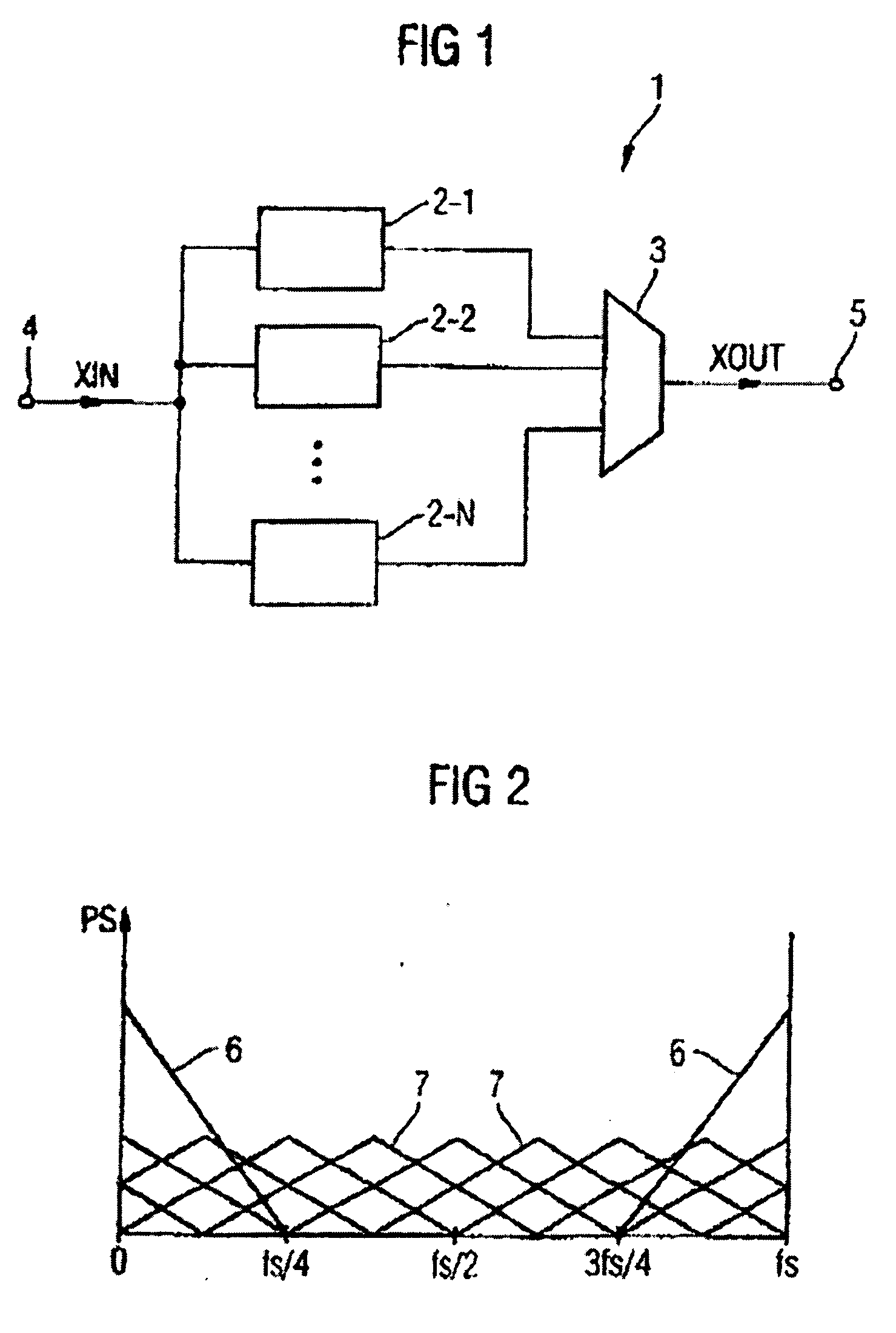
However, with such an array of individual ADCs 2-1 to 2-N there is a problem that any type of incorrect adaptation (mismatch) of the individual ADCs 2-1 to 2-N to one another leads to a conversion error which affects the output signal XOUT.
Especially at high frequencies, the intervals or timing differences of adjacent converters become smaller and smaller so that the time offset problem becomes more and more pronounced here.
In the same way, differences in the amplification of the input signal lead to undesired additional spectrums whose frequency is however dependent on the input signal.
Incorrect adaptations in the bandwidth of the individual parallel ADCs of the converter array typically give rise to undesired additional interference spectrums.
In particular, any form of deviation in the transmission behaviour and thus in the transmission function of the individual AD leads to additional undesired interference spectrums in the output signal.
However, this is undesired, in particular if the power of these additional spectrums 7 in the region of the input spectrum 6 is very large.
The problem of incorrect adaptation, and in particular the incorrect adaptation resulting from different time offset values increases with increasingly small structure sizes such as are used in future manufacturing technologies in what is referred to as the deep submicron range with structure widths of less than 70 nm since absolute errors have increasingly serious effects there owing to the smaller structural widths.
Analogue circuit measures for reducing incorrect adaptations entail a very high level of complexity

Method used


Image

  • Analog-to-digital converter operable with staggered timing
  • Analog-to-digital converter operable with staggered timing
  • Analog-to-digital converter operable with staggered timing

Examples


Embodiment Construction

[0054] Identical or functionally identical elements and signals are referred to with the same reference symbols in the figures of the drawing unless stated otherwise.

[0055] In FIG. 3, the circuit arrangement according to the invention is referred to by reference symbol 10. The circuit arrangement 10 contains a time interleaved analog-to-digital converter 11 which is connected at the input side to an input terminal 12 and at the output side to an output terminal 13. The analog-to-digital converter 11 has a converter array 14 which is composed in the present exemplary embodiment of four individual analog-to-digital converters 15-1 to 15-4 which are also referred to below as ADC channels 15-1 to 15-4. In FIG. 3, N=4 is therefore true. The individual analog-to-digital / convertors 15-1 to 15-4 are arranged in parallel with one another in the present exemplary embodiment, that is to say they are each connected at the input ends to the input 12 and at the output ends to the output 13 via a...


PUM


Abstract

An arrangement for a time interleaved analog-to-digital converter that converts an signal to a digital signal and has a converter array with a plurality of analog-to-digital converters arranged in a fixed sequence in parallel with one another and can be operated with staggered timing with respect to one another is disclosed. The arrangement has a connection network which, for the purposes of actuation with staggered timing, generates in each case one control signal for an individual analog-to-digital converter in each case, with the connection network predefining the time sequence with which the control signals actuate the individual analog-to-digital converters in such a way that owing to this sequence of the control signals and thus the sequence of the actuated individual analog-to-digital converters there is at least a reduction in an interference spectrum in the spectrum of the input and/or output signal. A sorting method for operating this analog-to-digital converter is also disclosed.

Description

PRIORITY AND CROSS REFERENCE TO RELATED APPLICATION [0001] This application claims priority to German Patent Application No. 10 2004 049 161.5, filed Oct. 8, 2004, which is incorporated by reference herein in its entirety. BACKGROUND OF THE INVENTION [0002] 1. Field of the Invention [0003] The invention relates to a time interleaved analog-to-digital converter, and to a sorting method for operating this analog-to-digital converter. [0004] 2. Description of the Related Art [0005] In modern data processing there is a need to process increasingly large amounts of data in shorter and shorter times and to condition it for further data communication. The respective electronic components, for example memory modules, processors and also logic components, such as PLDs or FPGAs, are therefore configured for increasingly high clock frequencies. As a result of this the analog-to-digital converters (ADC) which are present in such electronic components have correspondingly high sampling rates. [0...

Claims


Application Information

Patent Timeline
IPC IPC(8): H03M1/12
CPCH03M1/1215
Inventor DRAXELMAYR, DIETERKUBIN, GERNOTVOGEL, CHRISTIAN
Owner INFINEON TECH AG
Why Eureka
Try Eureka