Design method of semiconductor device and semiconductor device

a design method and semiconductor technology, applied in the direction of software simulation/interpretation/emulation, instruments, program control, etc., can solve the problems of reduced yield, insufficient redundant via conversion, and difficulty in achieving a miniaturized design pattern with high accuracy, so as to reduce the incidence of electromigration and improve the effect of efficiency

Inactive Publication Date: 2006-05-11
PANASONIC CORP
View PDF5 Cites 35 Cited by
  • Summary
  • Abstract
  • Description
  • Claims
  • Application Information

AI Technical Summary

Benefits of technology

[0014] According to the present invention, as many redundant vias as possible are inserted so that violations of a design constraint rule, except for a wire formation rule, such as an antenna effect error, a timing constraint violation and the like, can be avoided and a yield and a problem due to electromigration can be improved.
[0030] Specifically, according to the present invention, a redundant via provided in a location where a single via causes a problem at a high probability, e.g., a redundant via located at a short distance from another redundant via or a single via which causes reduction in yield or a redundant via located on a wire in which the incidence of electromigration is large, is given a higher priority. Then, redundant vias are converted to single vias, respectively, in descending order of priority. Thus, while a predetermined constraint violation such as an antenna effect error is taken into consideration, redundant vias can be efficiently provided. Accordingly, a cause of a problem due to an arrangement of a single via, e.g., reduction in yield and the occurrence of electromigration can be removed.
[0032] Specifically, according to the present invention, a single via provided in a location where a single via causes a problem at a high probability, e.g., a single via located at a short distance from a redundant via or another single via which causes reduction in yield or a single via located on a wire in which the incidence of electromigration is large, is given a higher priority. Then, single vias are converted to redundant vias, respectively, in descending order of priority. Thus, while a predetermined constraint violation such as an antenna effect error and a timing constraint violation is taken into consideration, redundant vias can be efficiently provided. Accordingly, a cause of a problem due to an arrangement of a single via, e.g., reduction in yield and the occurrence of electromigration can be removed.
[0033] Furthermore, in the semiconductor device of the present invention, for example, within a range where a predetermined constraint violation such as an antenna effect error and a timing constraint violation, each redundant via is provided in part in which a cause of reduction in yield and the like are removed by conversion from a single via. That is, each redundant via is provided on a wire having a structure in which electromigration tends to occur at high probability. Thus, under the consideration of an antenna effect error and a timing constraint violation, reduction in yield and the occurrence of electromigration can be resolved most effectively.

Problems solved by technology

In the recent miniaturization process, it is difficult to achieve a miniaturized design pattern with high accuracy in fabricating an LSI.
This results in reduction in yield.
Accordingly, there might be cases where redundant via conversion is not sufficiently performed.
However, in a known method, if redundant via conversion is performed to suppress reduction in fabrication yield due to electromigration, a violation of a specific constraint are increased.
As described above, due to a redundant via generated by conversion for improving problems with yield or electromigration, an antenna effect error occurs.
However, even though timing constraints are taken into consideration, in the case where a timing constraint violation might occur, as in U.S. Pat. No. 6,556,658, a method in which all vias are maintained as signal vias, i.e., single vias of which respective resultant redundant vias would not cause any problem are also left as single vias is not a sufficient measure for preventing reduction in yield.

Method used


Image

  • Design method of semiconductor device and semiconductor device
  • Design method of semiconductor device and semiconductor device
  • Design method of semiconductor device and semiconductor device

Examples


first embodiment

[0046] Hereinafter, a first embodiment of the present invention will be described with reference to the accompanying drawings.

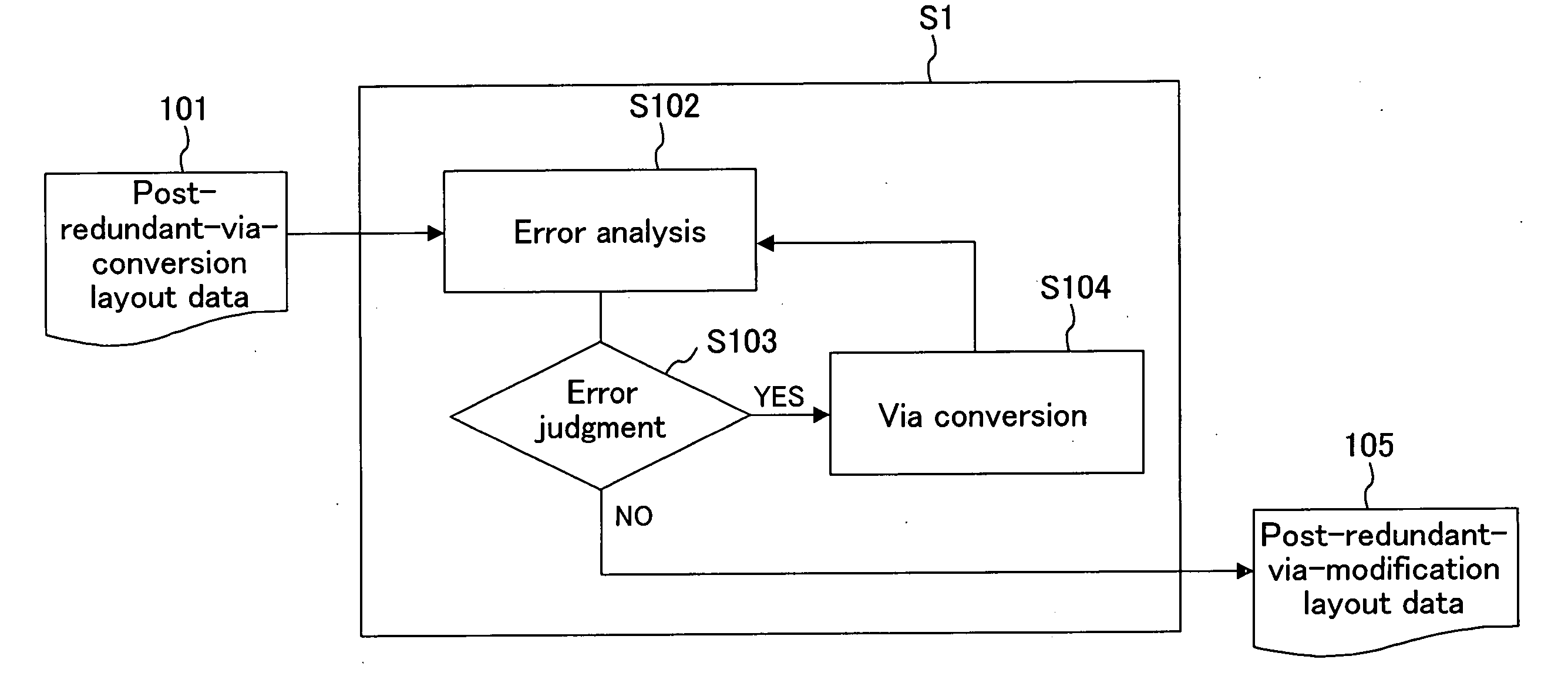
[0047]FIG. 1 is a diagram illustrating process steps performed by computer using a method for designing a semiconductor device according to the first embodiment of the present invention.

[0048] In FIG. 1, the reference numeral 101 denotes post-redundant-via-conversion layout data. Step S102 is the error analysis step of performing an error analysis for the post-redundant-via-conversion layout data 101 which has been input. Step S103 is the error judgment step of judging whether or not an error exists in a result of an error analysis of Step S102. Step S104 is the via conversion step of reconverting a redundant via to a single via when an error is found in the Step S103. The reference numeral 105 denotes layout data which is obtained after redundant via conversion and is to be output from the error judgment step S103 when an error is not found in the Step S10...

second embodiment

[0060] Hereinafter, a second embodiment of the present invention will be described with reference to the accompanying drawings.

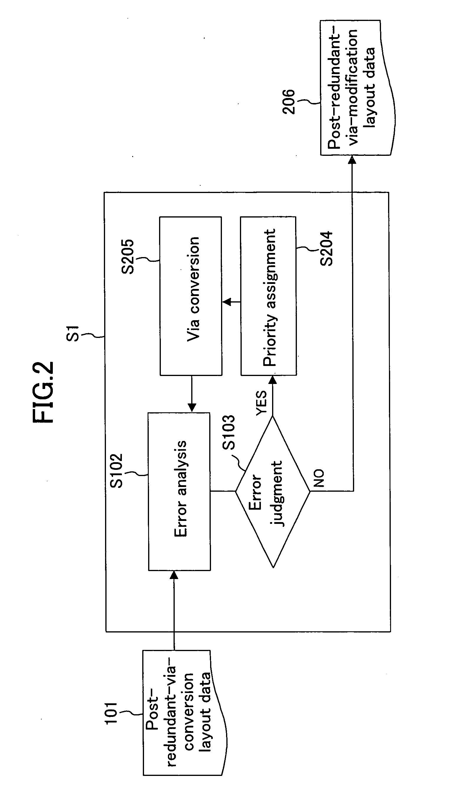
[0061]FIG. 2 is a diagram illustrating process steps using a method for designing a semiconductor device according to the second embodiment of the present invention.

[0062] In FIG. 2 illustrating this embodiment, as in FIG. 1 shown in the first embodiment, an error analysis for a timing constraint violation, an antenna effect error or the like is performed to post-redundant-via-conversion layout data 101 in the error analysis step S102 of the computer processing step 1 and an error judgment is performed for a result of the analysis in the error judgment step (judgment step) S103.

[0063] This embodiment is different from the first embodiment in that the priority assigning step (redundant via priority determination step) S204 of assigning priorities to errors such as an antenna effect error and a timing constraint violation caused by redundant vias being prov...

third embodiment

[0077] Hereinafter, a third embodiment of the present invention will be described with reference to the accompanying drawings.

[0078]FIG. 5 is a diagram illustrating process steps using a method for designing a semiconductor device according to the third embodiment of the present invention.

[0079] In FIG. 5, the reference numeral 501 denotes post-detail-routing layout data, Step S502 denotes the priority assigning step of assigning priorities in layout data after detail routing which has been input with respect to conversion of a single via to a redundant via, Step S503 denotes the via conversion step of converting a single via to a redundant via based on a result of priority assignment in the priority assigning step S502, and the reference numeral 504 denotes the post-redundant-via-conversion layout data output after conversion of a single via to a redundant via in the via conversion step S503. Among the above-described steps, the redundant via conversion step S505 including the pr...


PUM


Abstract

In an error analysis step, analysis of an antenna effect error, a timing constraint violation and the like is performed for layout data in which redundant via conversion has been performed. Then, whether or not an error exists is judged and, among redundant vias located on a signal line in which a design constraint violation has occurred, how many vias have to be converted to single vias, respectively, to avoid the design constraint violation is calculated. In a via conversion step, a redundant via which has caused an error is converted to a single via, based on a result of the calculation. Thus, a design constraint violation regarding an error such as an antenna effect error and a timing constraint violation caused by a redundant via obtained by converting a single via for improving yield hardly occurs.

Description

CROSS REFERENCE TO RELATED APPLICATIONS [0001] This non-provisional application claims priority under 35 U.S.C. § 119(a) on Patent Application No. 2004-323566 filed in Japan on Nov. 8, 2004, the entire contents of which are hereby incorporated by reference. BACKGROUND OF THE INVENTION [0002] The present invention relates to a design method of a semiconductor device and a semiconductor device which allow avoidance of violation of design constraints such as an antenna effect error and the like and insertion of as many redundant vias as possible in consideration of a yield, influences of electromigration and the like. [0003] In the recent miniaturization process, it is difficult to achieve a miniaturized design pattern with high accuracy in fabricating an LSI. This results in reduction in yield. [0004] The problem of reduction in yield can be improved by converting a single via connecting wiring patterns in different wiring layers to a set of two or more vias (the set of two or more vi...

Claims


Application Information

Patent Timeline
Patent Type & Authority Applications(United States)
IPC IPC(8): G06F17/50G06F9/45G06F9/455
CPCG06F17/5081G06F30/398
Inventor FUJITA, KAZUHISAKIMURA, FUMIHIROARAKI, TAKAYUKI
Owner PANASONIC CORP
Why Eureka
Try Eureka