Thin film transistor array panel and method for manufacturing the same

a technology of thin film transistors and array panels, which is applied in the direction of electrical equipment, semiconductor devices, instruments, etc., can solve the problems of poor adhesiveness of cu with glass substrates, difficult etching of cu, and limitation of application of cr to a large size lcd, etc., and achieves good reliability and low resistivity.

Active Publication Date: 2006-05-18
SAMSUNG DISPLAY CO LTD
View PDF7 Cites 127 Cited by
  • Summary
  • Abstract
  • Description
  • Claims
  • Application Information

AI Technical Summary

Benefits of technology

[0012] Accordingly, it would be desirable to solve the above mentioned problems and to provide a t

Problems solved by technology

Accordingly, there are limitations to applying Cr to a large size LCD.
However, the poor adhesiveness of Cu with

Method used


Image

  • Thin film transistor array panel and method for manufacturing the same
  • Thin film transistor array panel and method for manufacturing the same
  • Thin film transistor array panel and method for manufacturing the same

Examples


embodiment 1

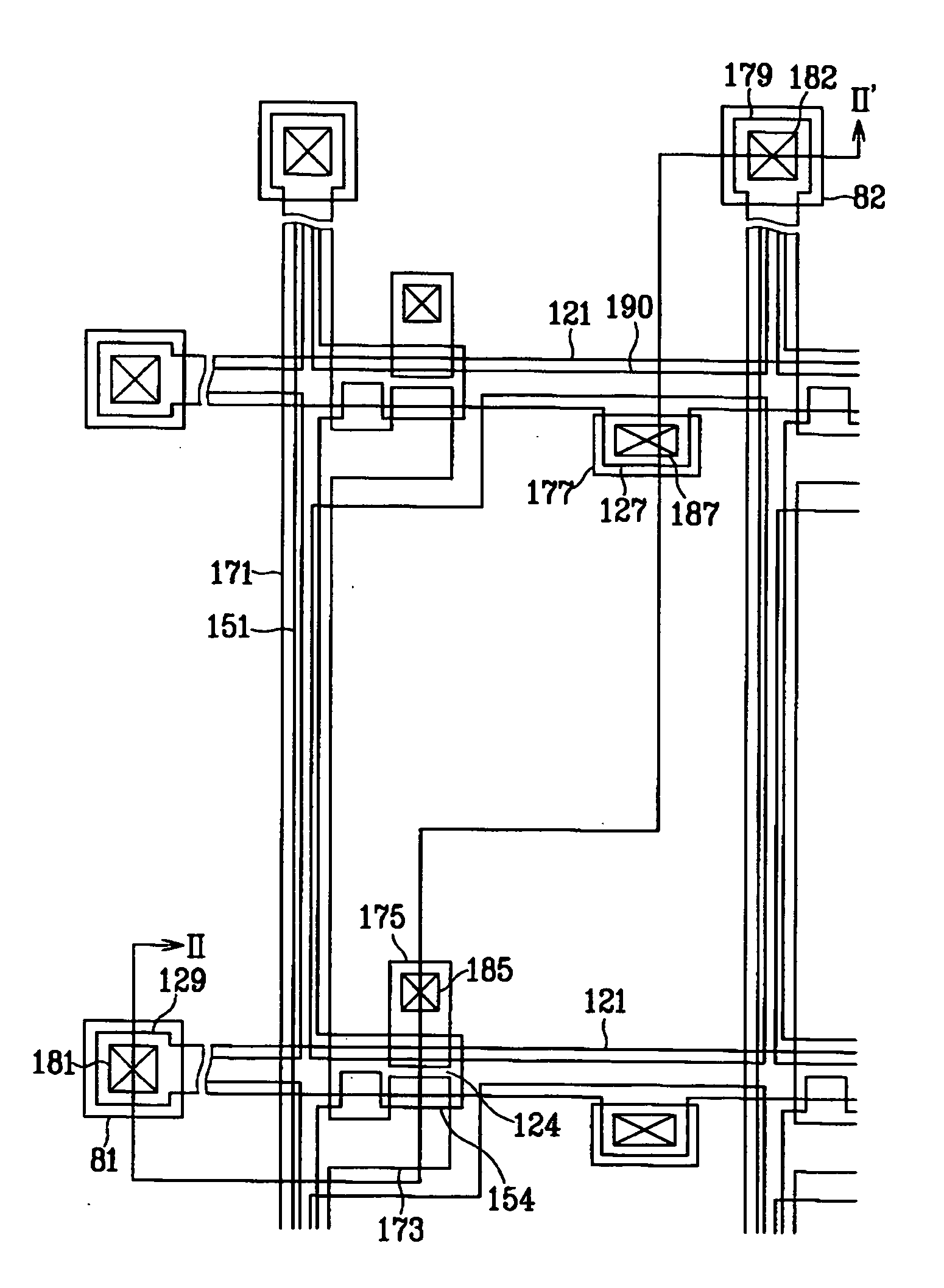
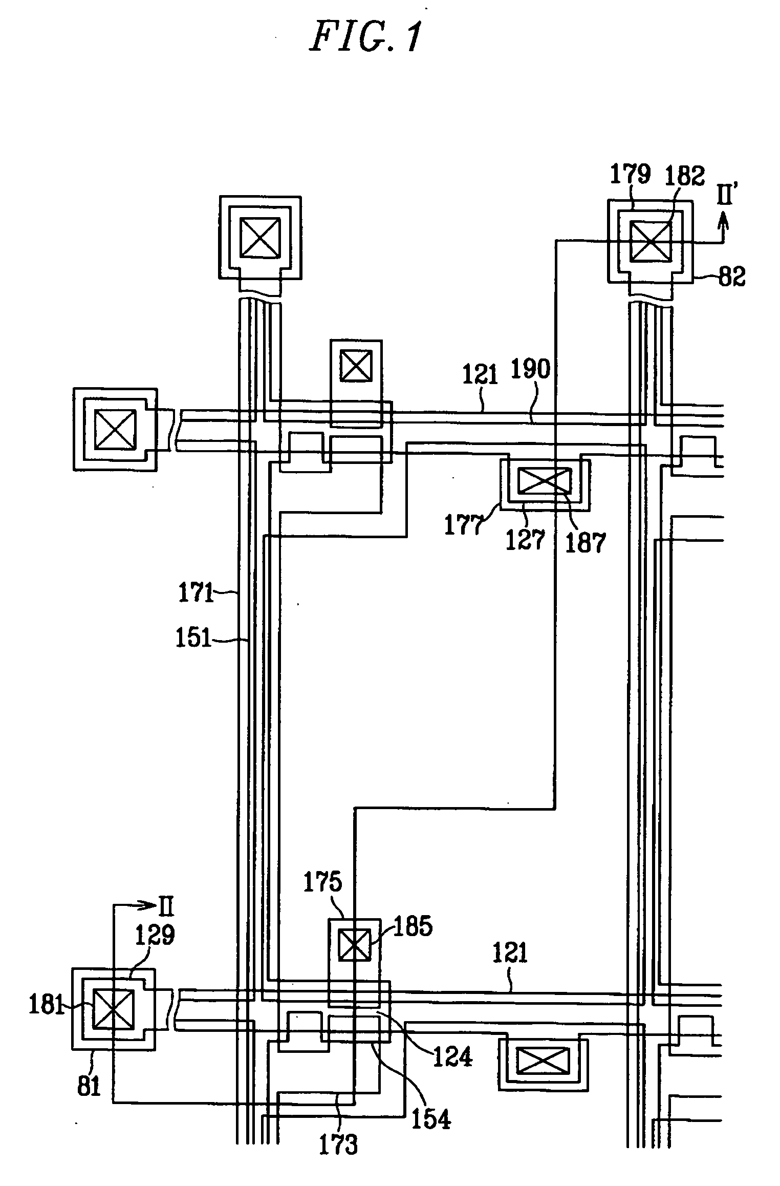
[0041] First, a TFT array panel for an LCD according to an embodiment of the present invention will be described in detail with reference to FIGS. 1 and 2.

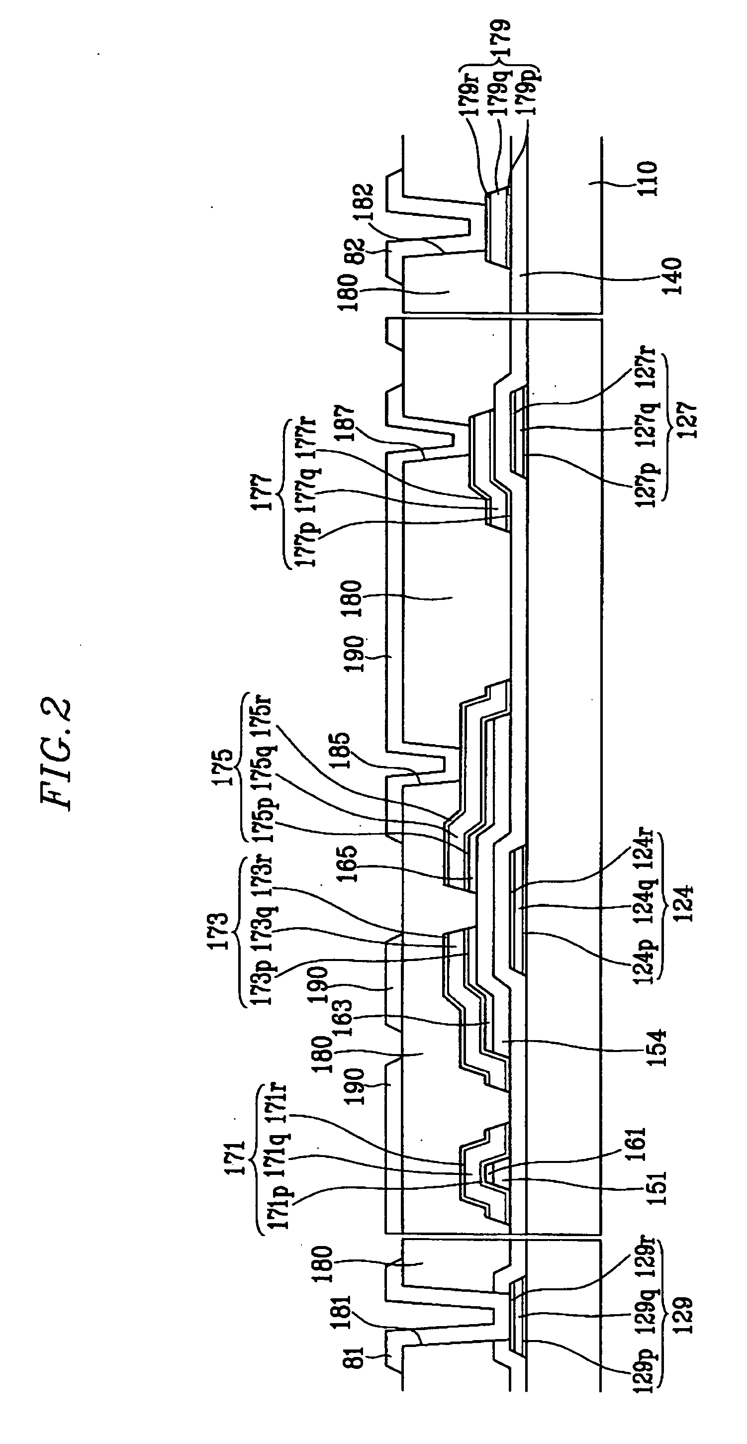
[0042]FIG. 1 is a layout view of a TFT array panel for an LCD according to an embodiment of the present invention, and FIG. 2 is a sectional view of the TFT array panel shown in FIG. 1 taken along the line II-II.

[0043] A plurality of gate lines 121 for transmitting gate signals are formed on an insulating substrate 110. The gate lines 121 are primarily formed in the horizontal direction and partial portions thereof form a plurality of gate electrodes 124. Also, different partial portions thereof that extend in a lower direction form a plurality of expansions 127. An end portion 129 of the gate line 121 has an expanded width for connection with an external device such as driving circuit.

[0044] The gate line 121 has first layers 124p, 127p, and 129p and second layers 124q, 127q, and 129q, and third layers 124r, 127r, and 129r. Th...

embodiment 2

[0103] Now, a TFT panel for an active matrix organic light emitting display (AM-OLED) according to another embodiment of the present invention will be described.

[0104]FIG. 7 is a layout view of a TFT array panel for an OLED according to another embodiment of the present invention. FIGS. 8A and 8B are sectional views of the TFT array panel shown in FIG. 7 taken along the line VIIIa-VIIIa′ and the line VIIb-VIIb′, respectively.

[0105] A plurality of gate conductors that include a plurality of gate lines 121, including a plurality of first gate electrodes 124a and a plurality of second gate electrodes 124b, are formed on an insulating substrate 110 such as transparent glass.

[0106] The gate lines 121 transmitting gate signals extend substantially in a transverse direction and are separated from each other. The first gate electrodes 124a protrude upward, as viewed from the perspective shown in FIG. 7. The gate lines 121 may extend to be connected to a driving circuit (not shown) integr...


PUM


Abstract

The present invention provides a thin film transistor array panel comprising an insulating substrate; a gate line formed on the insulating substrate; a gate insulating layer formed on the gate line; a drain electrode and a data line having a source electrode formed on the gate insulating layer, the drain electrode being adjacent to the source electrode with a gap therebetween; and a pixel electrode coupled to the drain electrode, wherein at least one of the gate line, the data line, and the drain electrode comprises a first conductive layer comprising a conductive oxide and a second conductive layer comprising copper (Cu).

Description

BACKGROUND [0001] (a) Field of the Invention [0002] The present description relates to a thin film transistor (TFT) array panel for a liquid crystal display (LCD) or an organic light emitting display (OLED), and a manufacturing method for the same. [0003] (b) Description of the Related Art [0004] Liquid crystal displays (LCDs) are one of the most widely used flat panel displays. An LCD includes a liquid crystal (LC) layer interposed between two panels provided with field-generating electrodes. The LCD displays images by applying voltages to the field-generating electrodes to generate an electric field in the LC layer that determines orientations of LC molecules therein to adjust the polarization of incident light. [0005] An LCD including two panels provided with field-generating electrodes respectively, wherein one panel has a plurality of pixel electrodes in a matrix and the other has a common electrode covering the entire surface of the panel, dominates the LCD market. [0006] The ...

Claims


Application Information

Patent Timeline
IPC IPC(8): H01L29/04
CPCH01L27/124H01L27/1214G02F1/136H01L27/1225
Inventor LEE, JE-HUNBAE, YANG-HOCHO, BEOM-SEOKJEONG, CHANG-OH
Owner SAMSUNG DISPLAY CO LTD
Why Eureka
Try Eureka