Coating support and method for the selective coating of conductive tracks on one such support

a technology of conductive pads and support posts, which is applied in the direction of electronic organic material coating, printed circuit non-printed electric components association, instruments, etc., can solve the problems of long and expensive techniques, wiring difficulties, and the inability to address conductive pads

Inactive Publication Date: 2006-05-18
ALCHIMER SA
View PDF5 Cites 24 Cited by
  • Summary
  • Abstract
  • Description
  • Claims
  • Application Information

AI Technical Summary

Problems solved by technology

This technique is long and expensive because it requires a mask to be put in place and removed for each type of lining material to be deposited.
However, a problem of addressing the conductive pads is posed.
The increase in the density of pads (number of pads per unit area) to be lined leads to the multiplication of the addressing contacts and leads to wiring difficulties.
This solution poses a first problem when the pads of a same family are uniformly spread out on the surface of the support (which is the case when the support groups together a series of identical components).
In this case, it is not possible for topological reasons to form different internal connections on a single surface.
Moreover, here again the increase in the density of the pads is limited by the multiplication of the internal connections.
Moreover, resorting to commutator or multiplexer means considerably increases the cost of the supports, in particular because it reduces the surface area available for the conductive pads.

Method used


Image

  • Coating support and method for the selective coating of conductive tracks on one such support
  • Coating support and method for the selective coating of conductive tracks on one such support
  • Coating support and method for the selective coating of conductive tracks on one such support

Examples


first embodiment

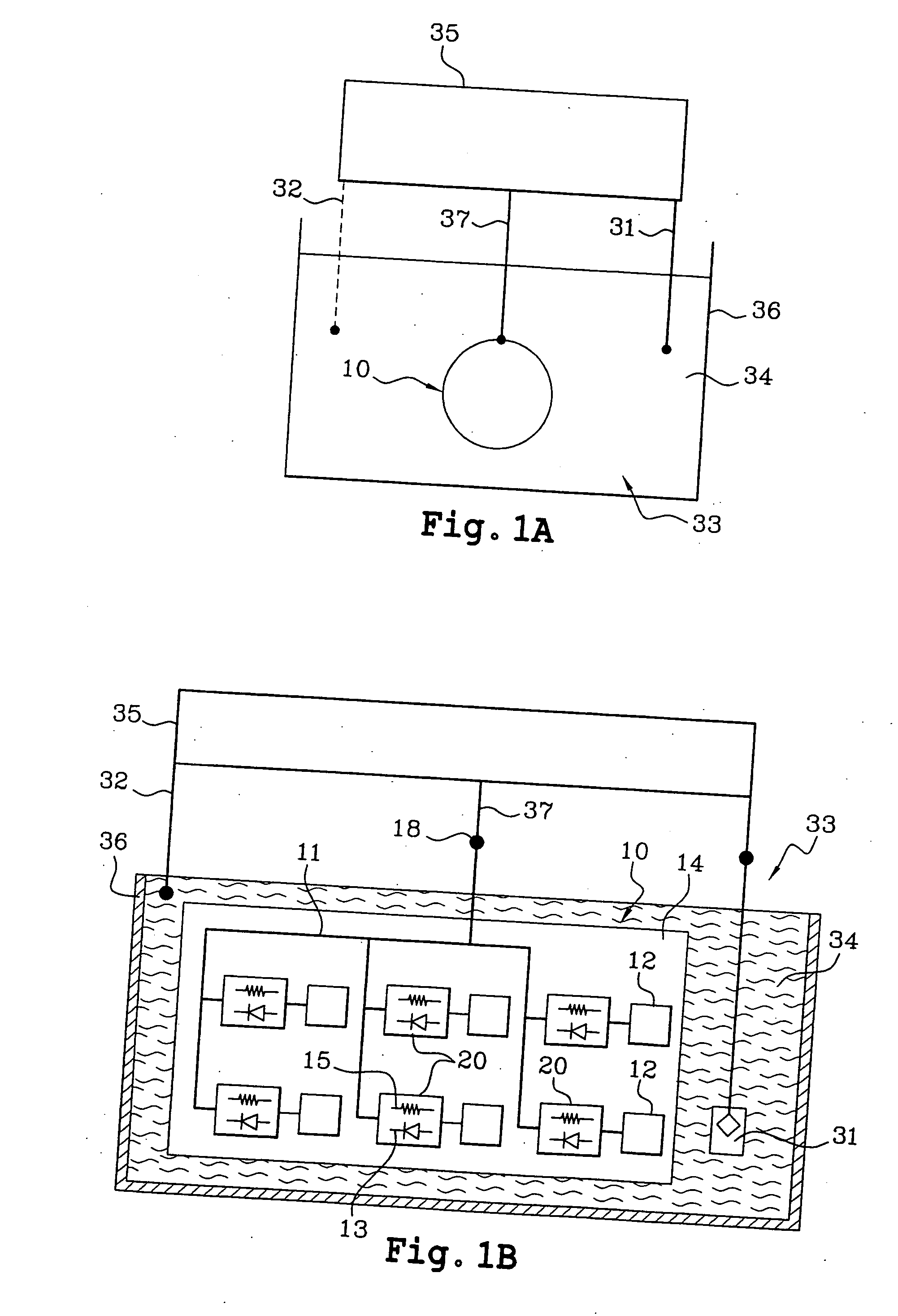
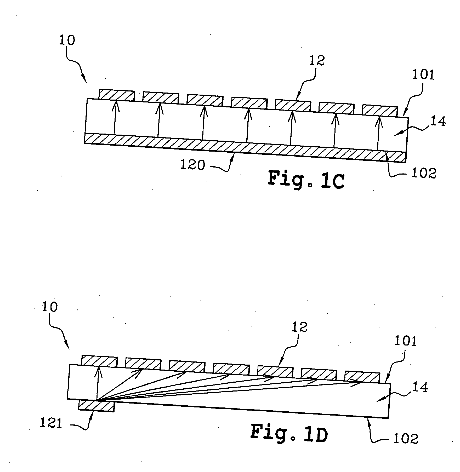
[0077] illustrated in FIG. 1C, the pad 18 is in the form of a conductive layer 120. It makes it possible to electrically connect all of the conductive pads 12 through the intermediary of a same access resistance due to the resistivity of the substrate 14, the pads 12 all being equidistant from the conductive plane 120. The application of a voltage to the shared addressing contact 120 makes it possible to apply an identical voltage on all of the conductive pads 12, simply lower due to the ohmic drop linked to the substrate (drop that may be compensated by the source applying the voltage to the shared addressing contact). An identical lining may thus be obtained on all of the conductive pads 12.

second embodiment

[0078] illustrated in FIG. 1D, the substrate 14 is resistive and the addressing contact 18 is in the form of a conductive plot 121 in a position not equidistant from the conductive pads 12. The substrate has a resistivity of a sufficient value to prevent the lining of at least one conductive pad 12 of the support under the application at the shared addressing contact 121 of a voltage allowing the lining of at least one other pad 12 of the support 10.

[0079]FIG. 2 is a diagram, more precisely a voltammogram, indicating on the Y-axis the evolution of an electrochemical current in the circuit 33 as shown in FIGS. 1a and 1b. The current is given as a function of a potential measured between a conductive pad 12 and reference electrode 32. This potential is shown on the X axis. This diagram therefore does not take account of the existence of the selection means 20 and therefore any difference between the potential applied by the potentiostat 35 and the potential obtained on the pad 12. Th...


PUM

PropertyMeasurementUnit
current densityaaaaaaaaaa
currentaaaaaaaaaa
thicknessaaaaaaaaaa

Abstract

The present invention concerns a lining support comprising a plurality of conductive pads ( 12 ) associated with a shared addressing contact ( 18 ) and means of selecting at least one pad to be lined by electrochemical means among the plurality of pads. In accordance with the invention, the selection means comprise means ( 20 ) of shifting a polarisation voltage, connected between the shared addressing contact and at least one pad to be addressed. Application to the lining of conductive pads.

Description

TECHNICAL FIELD [0001] The present invention concerns a support comprising conductive pads and a method of lining said pads by electrochemical means. Lining is taken to mean any deposition or attachment of a material at the surface of a pad of a support provided for this purpose. STATE OF THE PRIOR ART [0002] A technological background in the field of analysis supports covering various aspects of the invention is illustrated by documents (1) to (7), the references of which are detailed at the end of the present description. [0003] An example of support as envisaged in the invention is given by the substrate used for the collective manufacture of biological or chemical analysis supports, also known as “biochips” in the field of biology. This substrate comprises one or several identical biochips that each have a plurality of conductive pads used as test pads. After cutting the substrate, these pads, previously functionalised with reagents or “probe molecules”, are used to detect the p...

Claims


Application Information

Patent Timeline
Patent Type & Authority Applications(United States)
IPC IPC(8): H01L23/48G01N27/30C25D7/12C25D9/02G01N27/327G01N27/403G01N37/00
CPCB29C2043/5825C25D9/02C25D7/12
Inventor BUREAU, CHRISTOPHEPERRUCHOT, FRANCOISKERGUERIS, CHRISTOPHE
Owner ALCHIMER SA
Why Eureka
Try Eureka