Organic electroluminescent device

a technology of electroluminescent devices and electroluminescent tubes, which is applied in the direction of discharge tube luminescnet screens, natural mineral layered products, etc., can solve the problems of limiting the efficiency of processes in all the methods of manufacturing organic el devices, and preventing efficient mass production

Active Publication Date: 2006-05-18
SAMSUNG DISPLAY CO LTD
View PDF6 Cites 76 Cited by
  • Summary
  • Abstract
  • Description
  • Claims
  • Application Information

AI Technical Summary

Problems solved by technology

However, when producing a full-color element, the layers are deposited using a mask, which prevents efficient mass production (see U.S. Pat. Nos. 6,310,360, 6,303,238, and 6,097,147).
Thus, to manufacture organic EL devices according to a conventional method, R, G, and B must be separately micro-patterned, which is a limit to the efficiency of processes in all the methods of manufacturing organic EL devices.

Method used


Image

  • Organic electroluminescent device
  • Organic electroluminescent device
  • Organic electroluminescent device

Examples


example 1

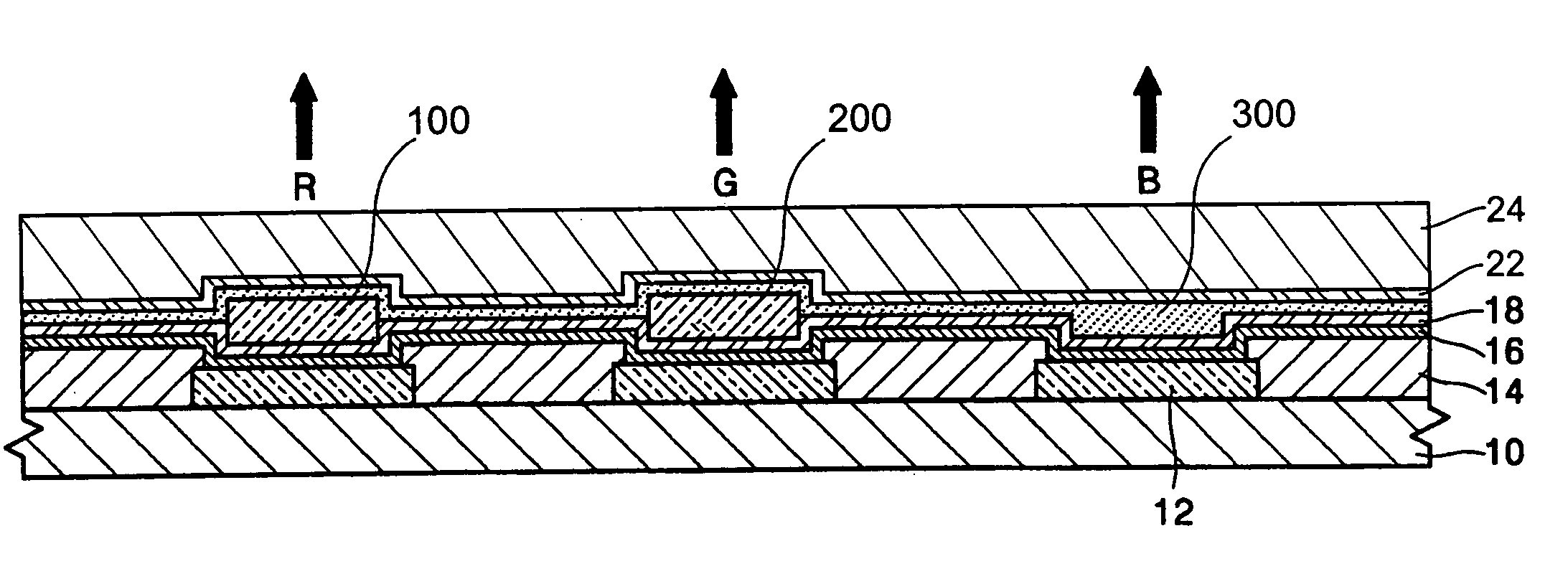
[0071] A hole injection layer (IDE 406, manufactured by Idemitsu Kosan Co., Ltd.) having a thickness of 30 nm and a hole transport layer (IDE 320, manufactured by Idemitsu Kosan Co., Ltd.) having a thickness of 30 nm were formed on a patterned test cell. Then, a host material composed of 90 parts by weight of 4,4′-N,N′-dicarbazole-biphenyl (CBP) (manufactured by UDC Co., Ltd.,) and 10 parts by weight of BAlq (Aluminum(III) bis(2-methyl-8-quinolinato)4-phenylpheolate), was doped with a dopant, (1-(phenyl)isoquinoline) iridium (III) acetylanetonate [Ir(piq)2acac], with a doping concentration of 10% by weight, and then layered to a thickness of 35 nm on the hole transport layer and patterned using LITI to obtain a phosphorescent light emitting layer. A blue fluorescent light emitting layer composed of IDE 140 (manufactured by Idemitsu Kosan Co., Ltd.) doped with IDE 105 (manufactured by Idemitsu Kosan Co., Ltd.), was formed to a thickness of 10 nm on the entire surface of the resultant...

example 2

[0072] An organic EL device was manufactured in the same manner as in Example 1, except that 75 parts by weight of CBP and 25 parts by weight of BAlq were used to form a phosphorescent light emitting layer.

example 3

[0073] An organic EL device was manufactured in the same manner as in Example 1, except that 50 parts by weight of CBP and 50 parts by weight of BAlq were used to form a phosphorescent light emitting layer.


PUM

PropertyMeasurementUnit
HOMOaaaaaaaaaa
HOMOaaaaaaaaaa
HOMOaaaaaaaaaa

Abstract

An organic electroluminescent (EL) device which has a light emitting layer composed of at least one phosphorescent dopant disposed between a first electrode and a second electrode; and a blue light emitting layer contacting the light emitting layer, wherein the light emitting layer has a hole transport material and an electron transport material as a host.

Description

CLAIM OF PRIORITY [0001] This application claims the benefit of Korean Patent Application No. 10-2004-0092637, filed on Nov. 12, 2004, in the Korean Intellectual Property Office, the disclosure of which is incorporated herein in its entirety by reference. BACKGROUND OF THE INVENTION [0002] 1. Field of the Invention [0003] The present invention relates to an organic electroluminescent (EL) device, and more particularly, to an organic EL device including a blue light emitting layer which contacts red and green light emitting layers. [0004] 2. Description of the Related Art [0005] Organic EL devices typically comprise a plurality of layers, such as a first electrode, a second electrode, a hole injection layer, a hole transport layer, a light emitting layer, an electron transport layer, an electron injection layer, etc. Organic EL devices may be produced using a polymer material or a small molecule material. In a small molecule organic EL device, layers are formed by vacuum deposition. ...

Claims


Application Information

Patent Timeline
Patent Type & Authority Applications(United States)
IPC IPC(8): H01L51/52H05B33/12
CPCH01L27/3211H01L51/0052H01L51/0062H01L51/0081Y10S428/917H01L51/5016H01L51/5096H01L51/56H01L51/0085H10K59/35H10K85/615H10K85/649H10K85/324H10K85/342H10K50/11H10K2101/10H10K50/18H10K71/00C09K11/06
Inventor LEE, JUN-YEOBCHUN, MIN-SEUNGCHOI, YONG-JOONG
Owner SAMSUNG DISPLAY CO LTD
Why Eureka
Try Eureka