Mixed electrical and optical LGA interposer for facilitating chip to board communications by dual signal types

Active Publication Date: 2006-05-18
GLOBALFOUNDRIES US INC
View PDF8 Cites 12 Cited by
  • Summary
  • Abstract
  • Description
  • Claims
  • Application Information

AI Technical Summary

Problems solved by technology

Mixed signal types, however, pose significant packaging challenges.
However, the omission of a compliant window would allow introduction of dust which could block the optical path and lead to reliability concerns.

Method used


Image

  • Mixed electrical and optical LGA interposer for facilitating chip to board communications by dual signal types
  • Mixed electrical and optical LGA interposer for facilitating chip to board communications by dual signal types
  • Mixed electrical and optical LGA interposer for facilitating chip to board communications by dual signal types

Examples


Embodiment Construction

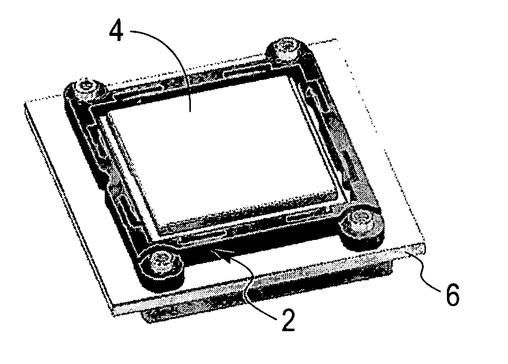
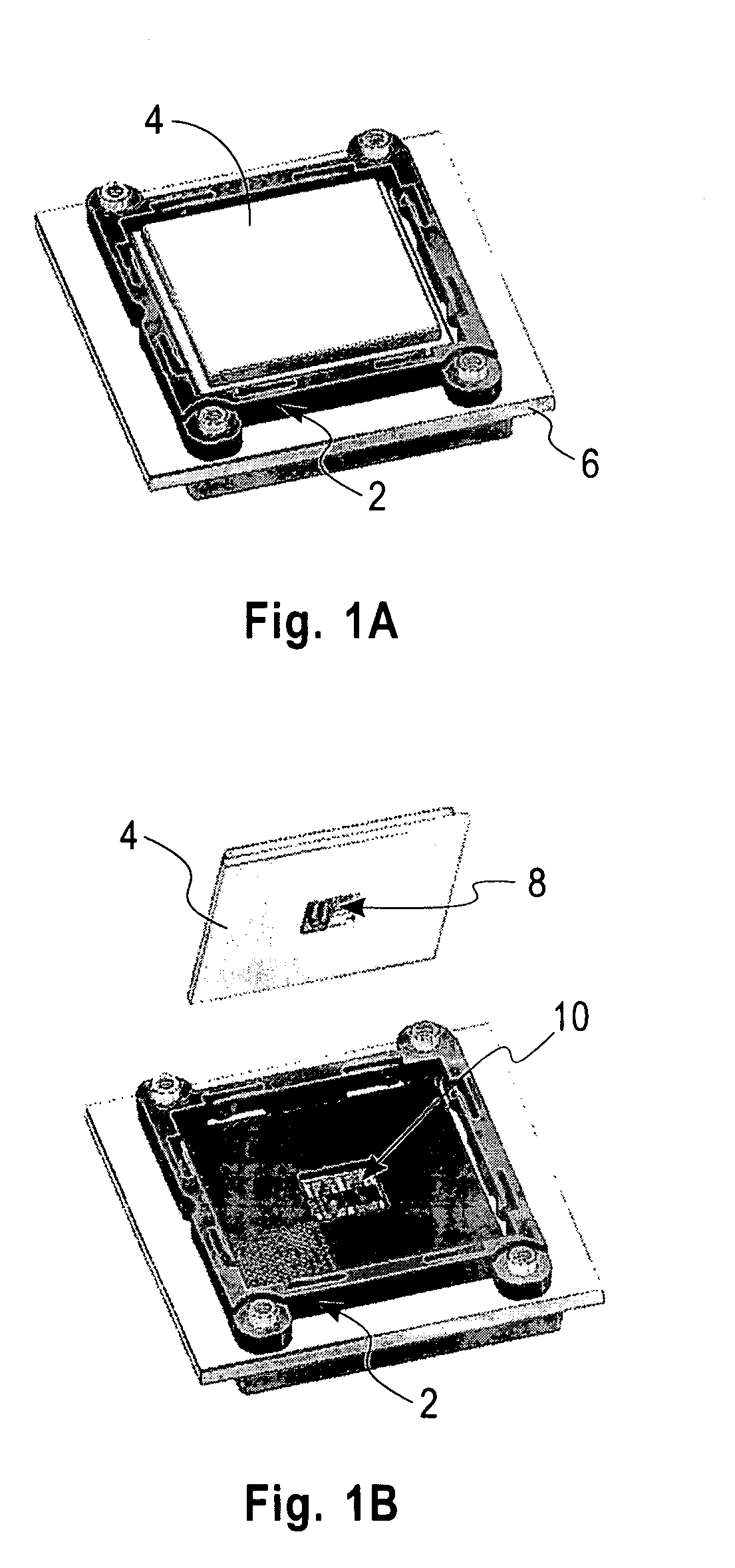
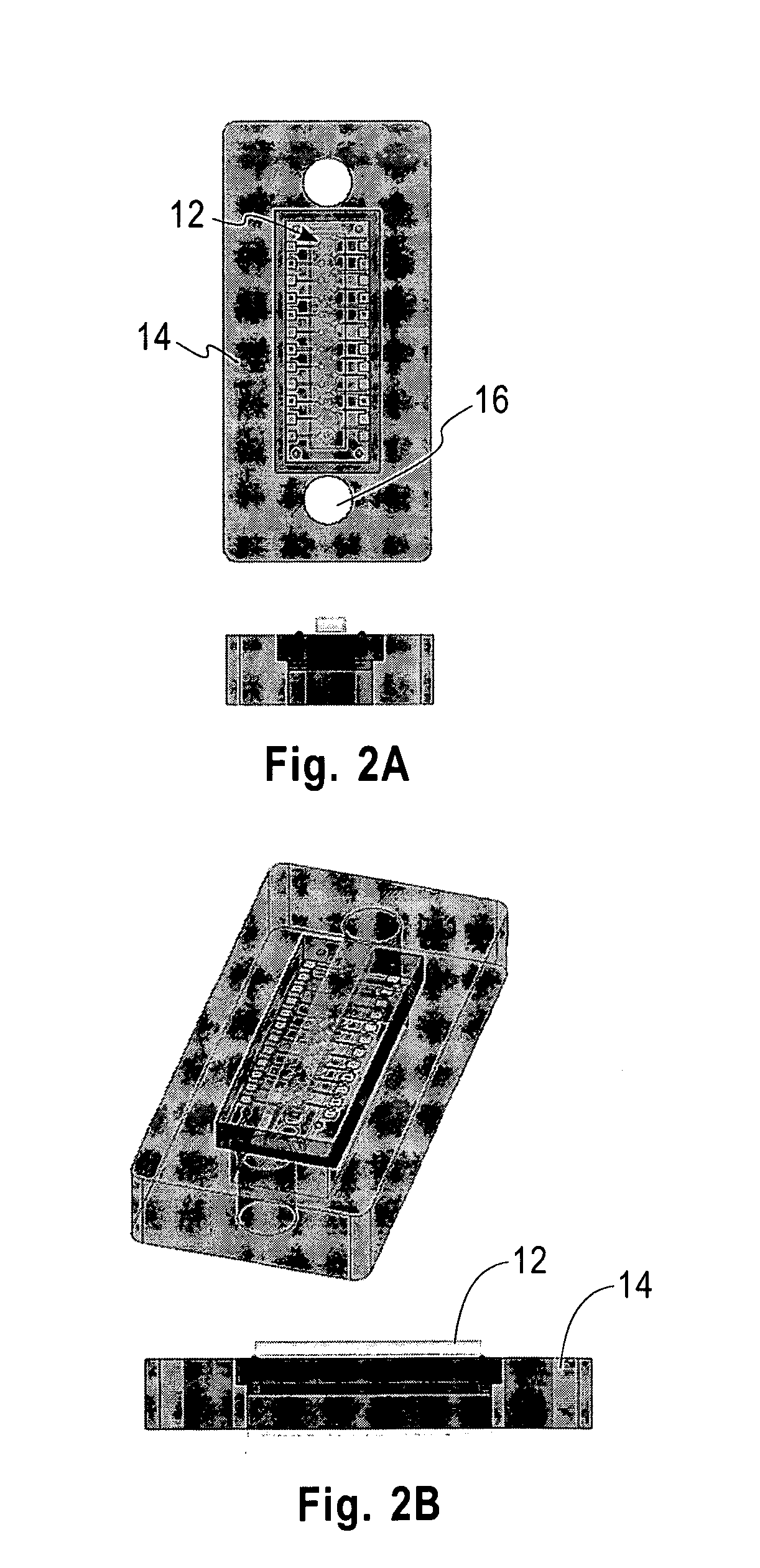
[0006] An electronic package consisting of a chip or a plurality of chips mounted to a chip-carrier such as a multichip ceramic, glass ceramic or organic module and which also has embedded in this module arrays of vertical cavity Semiconductor Cavity Laser (VCSCL) and photodetectors (PD), is connected via the application of pressure from appropriate hardware to a printed wiring board via a land grid array interposer which can accommodate both electrical and optical signals. Some lens assemblies may also be required. In addition to the electrical signals which are passed from BLM to the LGA contacts and through to the PWB, as in an ordinary electrical LGA, optical signals are passed from the VCSCL and PD array in the module, through the optical window in the LGA to the corresponding VCSCL and PDs on the PWB.

[0007]FIG. 1 illustrates an example of such an arrangement but does not show the details of the optical window, for which there are many possible designs. FIG. 2 illustrates the ...


PUM


Abstract

Integrated optoelectronic chips or collections of chips on a module that have both electrical as well as optical interconnects offer many advantages in speed, power consumption and heat generation. Mixed signal types, however, pose significant packaging challenges. This invention describes a land grid array (LGA) interposer which can simultaneously connect electrical and optical signals from a module to a printed circuit board.

Description

BACKGROUND [0001] Integrated optoelectronic chips or collections of chips on a module that have both electrical as well as optical interconnects offer many advantages in speed, power consumption and heat generation. Mixed signal types, however, pose significant packaging challenges. This invention describes a land grid array (LGA) interposer which can simultaneously connect electrical and optical signals from a module to a printed circuit board. [0002] In a mixed optical electrical LGA interposer (OELGA) there are a plurality of electrical contacts which are constructed to have conducting elements extend in both directions perpendicular to the plane of the interposer with the purpose of connecting a BLM from a module above to the TLM of a PWB below. These conducting elements or contacts (aka buttons) can be composed of a variety of materials and geometries but always have both conducting and mechanical compliance (spring) functions. There are also one or more optical interconnects (...

Claims


Application Information

Patent Timeline
IPC IPC(8): H01R13/62
CPCG02B6/43
Inventor HOUGHAM, GARETH G.BUDD, RUSSELL A.CHINIWALLA, PUNIT P.COTEUS, PAUL W.LANZETTA, ALPHONSO P.LIBSCH, FRANK R.
Owner GLOBALFOUNDRIES US INC
Why Eureka
Try Eureka