Organic thin film transistor, method of manufacturing the same, and flat panel display device with the organic thin film transistor

a thin film transistor and organic technology, applied in the field of organic thin film transistors, can solve the problems of high manufacturing cost, easy breakage, high contact resistance between an organic semiconductor layer and a source and drain electrode, and achieve good adhesiveness and contact resistan

Inactive Publication Date: 2006-05-25
SAMSUNG DISPLAY CO LTD
View PDF5 Cites 67 Cited by
  • Summary
  • Abstract
  • Description
  • Claims
  • Application Information

AI Technical Summary

Benefits of technology

[0011] It is yet an object of the present invention to provide an organic thin film transistor which has good adhesiveness, good contact resistance as well as allows ohmic contact between an organic semiconductor layer and a source electrode and a drain electrode, and a manufacturing method thereof and a flat panel display device using the organic thin film transistor.

Problems solved by technology

Such silicon thin film transistor has disadvantages in that the manufacturing cost is high, and it can be easily broken by external impact, and it cannot be formed on a flexible plastic substrate because formation thereof requires a high temperature process of over 300° C.
However, since the organic thin film transistor can not separately form a region doped with high density impurities, it has a disadvantage in that the contact resistance between an organic semiconductor layer and a source and drain electrodes is high.
However, such noble metals for the source and drain electrodes are expensive.
In addition, since their adhesiveness to the organic semiconductor layer is poor, there is a high probability of failure and there is a short life span.
Moreover, since such noble metals have very poor adhesiveness also to a gate insulating layer, a separate adhesive layer is additionally required.

Method used


Image

  • Organic thin film transistor, method of manufacturing the same, and flat panel display device with the organic thin film transistor
  • Organic thin film transistor, method of manufacturing the same, and flat panel display device with the organic thin film transistor
  • Organic thin film transistor, method of manufacturing the same, and flat panel display device with the organic thin film transistor

Examples


first embodiment

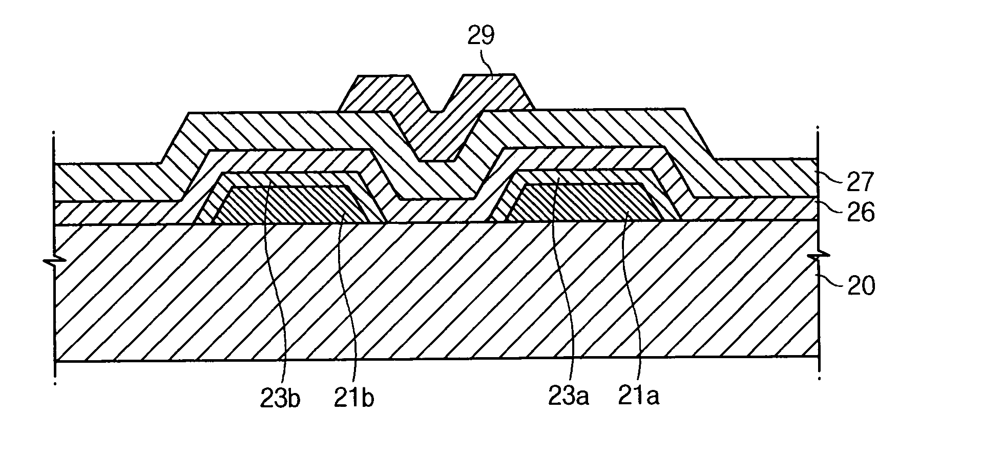
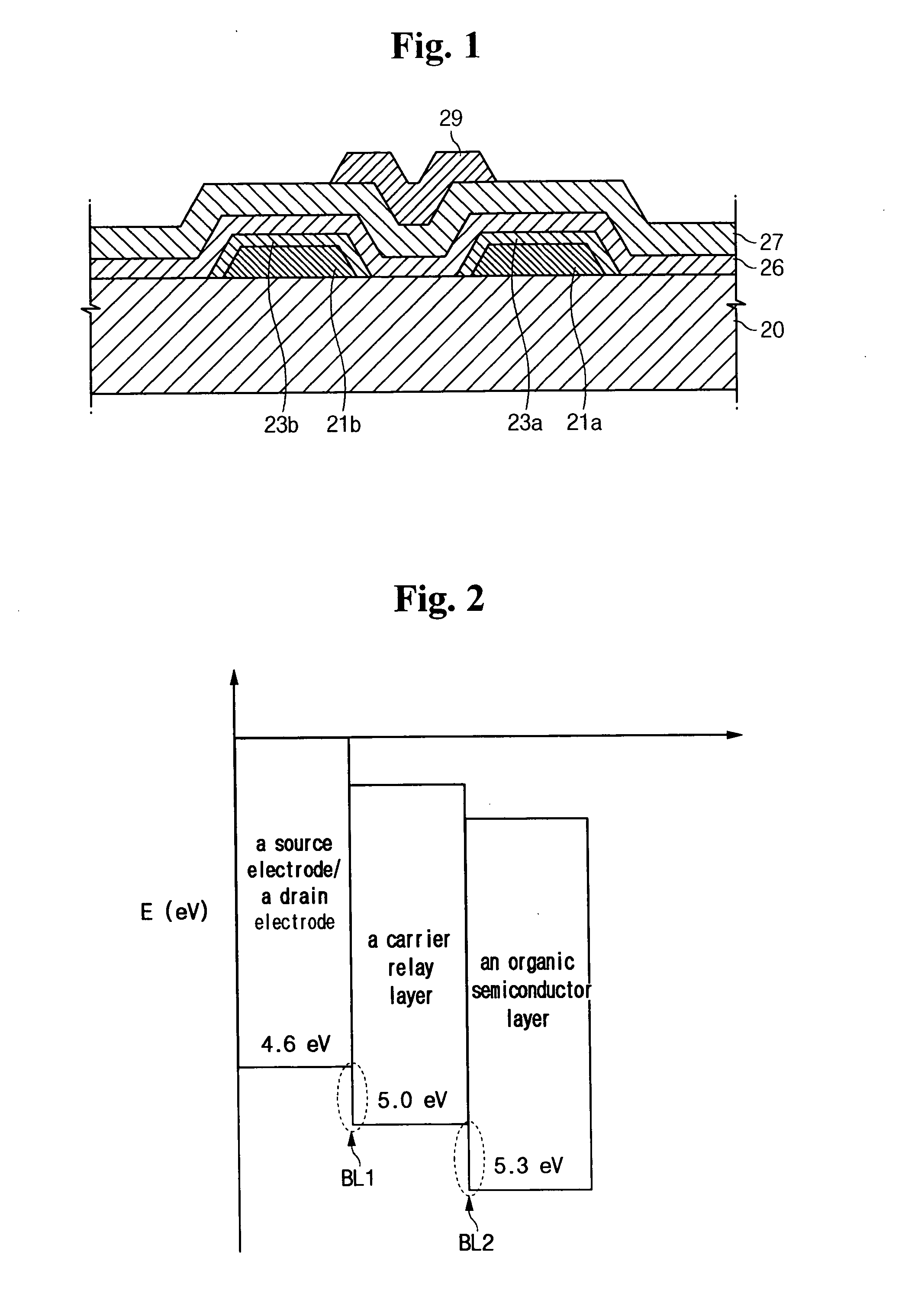
[0041] Turning now to the figures, FIG. 1 is a cross sectional view of an organic thin film transistor according to the present invention. As shown in FIG. 1, a source electrode 21a and a drain electrode 21b are formed on a substrate 20, and carrier relay layers 23a and 23b and an organic semiconductor layer 26 are sequentially formed covering the source electrode 21a and the drain electrode 21b. Accordingly, the carrier relay layers 23a and 23b are located between the source and drain electrodes 21a and 21b and the organic semiconductor layer 26. A gate insulating layer 27 is formed covering the organic semiconductor layer 26, and a gate electrode 29 is formed on the gate insulating layer 27 between the source and drain electrodes 21a and 21b.

[0042] The details of the organic thin film transistor of FIG. 1 are as follows. The substrate 20 can be made of glass, silicon, plastic, or metal. The plastic can be polyethylene terephthalate (PET), polyethylene naphtahlate (PEN), polyether...

second embodiment

[0092]FIGS. 12a to 12d are cross sectional views of the organic thin film transistor to sequentially illustrate a manufacturing method thereof according to the present invention. As shown in FIG. 12a, the source electrode 121a and the drain electrode 121b are formed on the substrate 120. A hydrophobic material layer 124c is formed on the entire surface of the substrate 120 to cover the source electrode 121a and the drain electrode 121b.

[0093] The source electrode 121a and the drain electrode 121b can be formed by vapor depositing on the entire surface of the substrate 120 to form a conductive layer and then patterning the conductive layer. Alternatively, the source electrode 121a and the drain electrode 121b can be formed by forming a patterned conductive layer on the substrate 120 using a mask. Alternatively, source electrode 121a and drain electrode 121b can be formed by inkjet printing, etc.

[0094] In addition, the hydrophobic material layer 124c can be formed by applying hydrop...


PUM

PropertyMeasurementUnit
resistivityaaaaaaaaaa
temperatureaaaaaaaaaa
work functionaaaaaaaaaa

Abstract

An organic thin film transistor that has good adhesiveness and good contact resistance as well as allows ohmic contact between an organic semiconductor layer and a source electrode and a drain electrode, and its manufacturing method. There is also provided a flat panel display device using the organic thin film transistor. The organic thin film transistor includes a source electrode, a drain electrode, an organic semiconductor layer, a gate insulating layer, and a gate electrode formed on a substrate, and a carrier relay layer including conductive polymer material formed at least between the organic semiconductor layer and the source electrode or the organic semiconductor layer and the drain electrode.

Description

CLAIM OF PRIORITY [0001] This application makes reference to, incorporates the same herein, and claims all benefits accruing under 35 U.S.C. §119 from an applications earlier filed in the Korean Intellectual Property Office on 23 Nov. 2004, 24 Oct. 2005, and 3 Nov. 2005 and there duly assigned Serial Nos. 10-2004-0096210, 10-2005-0100278, and 10-2005-0104925, respectively. BACKGROUND OF THE INVENTION [0002] 1. Field of the Invention [0003] The present invention relates to an organic thin film transistor, a method of manufacturing the same, and a flat panel display device with the same, and more particularly, to an organic thin film transistor with an improved structure, a method of manufacturing the same, and a flat panel display device with the same. [0004] 2. Description of the Related Art [0005] Generally, a silicon thin film transistor includes a source region and a drain region doped with high-density impurities, a semiconductor layer having a channel region formed between the ...

Claims


Application Information

Patent Timeline
Patent Type & Authority Applications(United States)
IPC IPC(8): H01L29/08
CPCB82Y30/00H01L51/0036H01L51/0037H01L51/0052H01L51/0078H01L51/0516H01L51/0541H01L51/0545H01L51/105H10K85/1135H10K85/113H10K85/615H10K85/311H10K10/468H10K10/464H10K10/84H10K10/466
Inventor AHN, TAEKSUH, MIN-CHULKOO, JAE-BONPARK, JIN-SEONG
Owner SAMSUNG DISPLAY CO LTD
Why Eureka
Try Eureka