Supercharge Your Innovation With Domain-Expert AI Agents!

Apparatus and method for treating surfaces of semiconductor wafers using ozone

a technology of ozone treatment and surface treatment, applied in the direction of cleaning process and apparatus, chemistry apparatus and process, cleaning liquid, etc., can solve the problems of ozone concentration, inability to use heated processing fluid and/or processing fluid having certain chemicals, etc., and achieve the effect of reducing the thickness of the boundary layer

Inactive Publication Date: 2006-06-01
JEONG IN KWON +2
View PDF6 Cites 18 Cited by
  • Summary
  • Abstract
  • Description
  • Claims
  • Application Information

AI Technical Summary

Benefits of technology

This approach significantly increases the concentration of ozone reaching the wafer surface, improving the cleaning and oxide growth processes by promoting more effective oxidation reactions.

Problems solved by technology

Consequently, the use of heated processing fluid and / or processing fluid having certain chemicals may not be practical, although such processing fluid may be preferred, due to the high ozone decay rate, which significantly reduces the concentration of ozone applied to the wafer surface.

Method used


Image

  • Apparatus and method for treating surfaces of semiconductor wafers using ozone
  • Apparatus and method for treating surfaces of semiconductor wafers using ozone
  • Apparatus and method for treating surfaces of semiconductor wafers using ozone

Examples


first embodiment

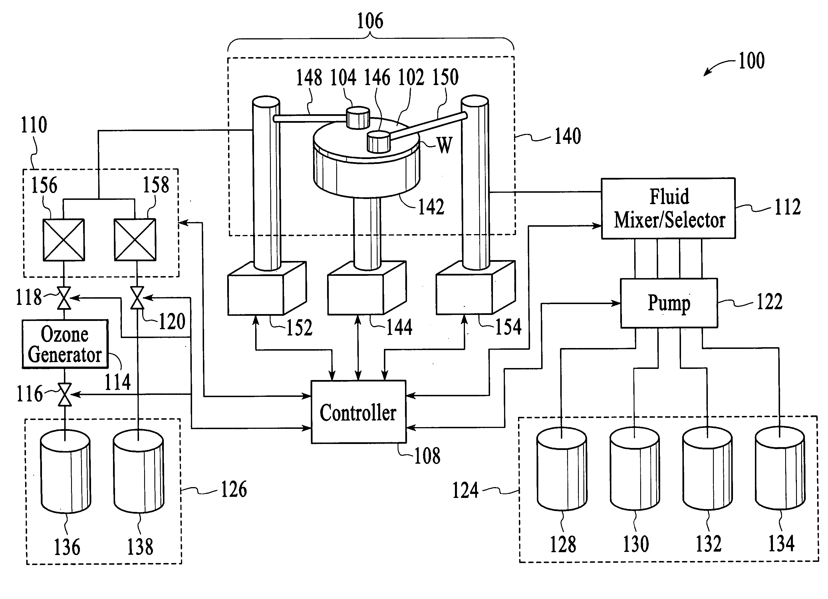
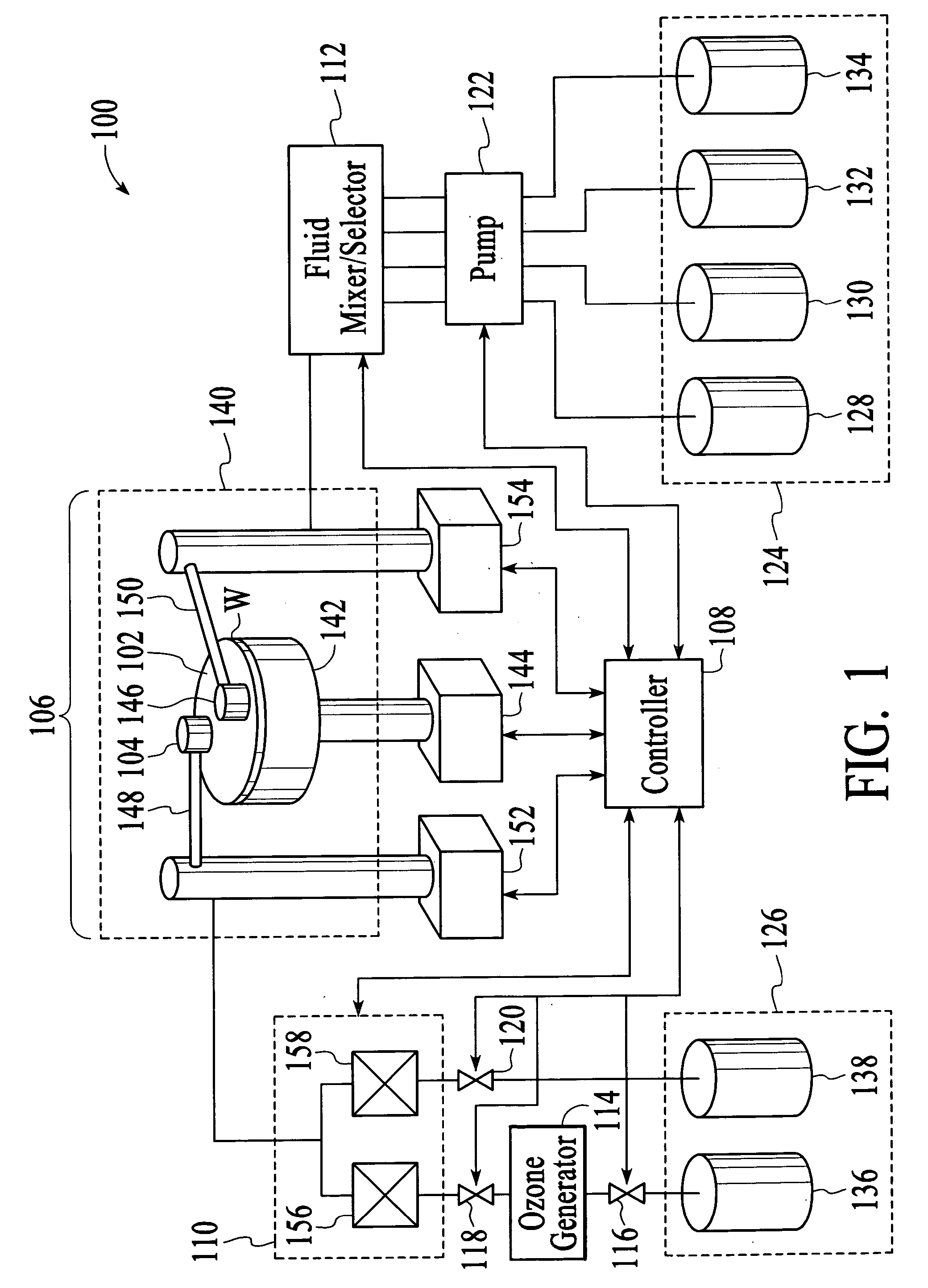
[0040] With reference to FIG. 1, an apparatus 100 for treating a surface 102 of a semiconductor wafer W using a processing fluid in conjunction with a reactive gaseous agent, such as ozone gas, to cause a desired reaction of materials on the wafer surface, such as oxidation, in accordance with the invention is shown. Thus, the apparatus 100 can be used to remove oxidizable materials on the wafer surface and / or to form an oxide layer on the wafer surface, which may be used as a passivation or interfacial layer for a semiconductor device. The apparatus 100 uses streams of reactive gaseous agent ejected from a gas nozzle structure 104 to increase the amount of reactive gaseous agent to reach the semiconductor wafer surface through a boundary layer of processing fluid formed on the wafer surface. As described in more detail below, the amount of reactive gaseous agent to reach the semiconductor wafer surface is increased either by creating depressions at different locations on the bounda...

second embodiment

[0061] Turning now to FIG. 18, an apparatus 1800 for treating a surface of a semiconductor wafer, e.g., the semiconductor wafer W, using a processing fluid in conjunction with a reactive gaseous agent, such as ozone, to cause a desired reaction of materials on the wafer surface, such as oxidation, in accordance with the invention is shown. The same reference numerals of FIG. 1 are used to identify similar elements in FIG. 18. Similar to the apparatus 100 of FIG. 1, the apparatus 1800 can be used to remove oxidizable materials on the wafer surface and / or to form an oxide layer on the wafer surface, which may be used as a passivation or interfacial layer for a semiconductor device. However, in contrast to the apparatus 100, the apparatus 1800 uses streams of inert gas in addition to streams of reactive gas to create depressions on a boundary layer of processing fluid to reduce the thickness of the boundary layer or to create holes through the boundary layer to expose portions of the w...


PUM


Abstract

An apparatus and method for treating surfaces of semiconductor wafers with a reactive gas, such as ozone, utilizes streams of gaseous material ejected from a gas nozzle structure to create depressions on or holes through a boundary layer of processing fluid formed on a semiconductor wafer surface to increase the amount of reactive gas that reaches the wafer surface through the boundary layer. The apparatus and method may be used to clean a semiconductor wafer surface and / or grow an oxide layer on the wafer surface by oxidation.

Description

CROSS REFERENCE TO RELATED APPLICATION [0001] The present application is a continuation of copending application Ser. No. 10 / 350,739 filed on Jan. 23, 2003, which is a continuation-in-part of prior application Ser. No. 10 / 282,562 filed on Oct. 29, 2002. The entire disclosure of the copending application Ser. No. 10 / 350,739 is incorporated herein by reference.FIELD OF THE INVENTION [0002] The invention relates generally to semiconductor fabrication processing, and more particularly to an apparatus and method for treating surfaces of semiconductor wafers using ozone. BACKGROUND OF THE INVENTION [0003] Recently, the use of ozone has attracted much attention in the semiconductor fabrication industry. Ozone has been found to be effective in cleaning a surface of a semiconductor wafer by oxidizing undesirable organic and / or metallic materials, such as photoresist residue, which can then be removed from the wafer surface. Depending on the cleaning process, a layer of oxide may be formed on...

Claims


Application Information

Patent Timeline
Patent Type & Authority Applications(United States)
IPC IPC(8): B08B3/00B08B3/02B08B3/08B08B3/12B08B7/04H01LH01L21/00H01L21/302H01L21/306H01L21/31H01L21/316H01L21/461H01L21/469
CPCB08B3/02B08B3/08B08B2203/005H01L21/67051H01L21/02238H01L21/31662H01L21/02046
Inventor JEONG, IN KWONKIM, YONG BAEKIM, JUNGYUP
Owner JEONG IN KWON
Features
  • R&D
  • Intellectual Property
  • Life Sciences
  • Materials
  • Tech Scout
  • Unparalleled Data Quality
  • Higher Quality Content
  • 60% Fewer Hallucinations
Learn More