Magnetoresistance element, magnetic memory, and magnetic head
a technology of magnetic memory and magnetic head, which is applied in the manufacture of flux-sensitive heads, instruments, record information storage, etc., can solve the problems of shortened wiring life and increased power consumption
- Summary
- Abstract
- Description
- Claims
- Application Information
AI Technical Summary
Problems solved by technology
Method used
Image
Examples
example 1
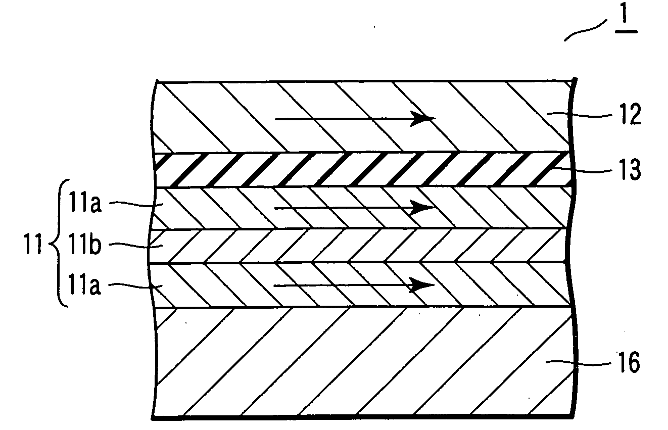
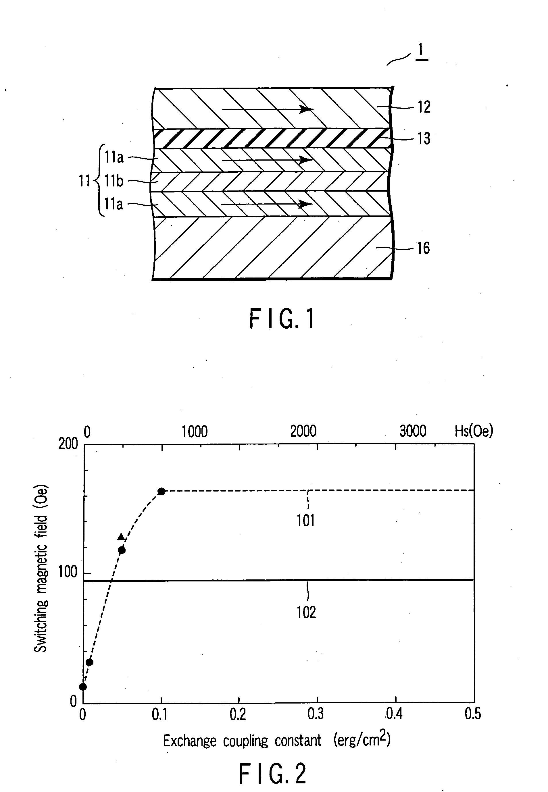
[0080]FIG. 6 is a cross-sectional view schematically showing a magnetoresistance element 1 according to Example 1 of the present invention. The magneto-resistance element 1 shown in FIG. 6 is a spin valve type tunnel junction element (MTJ element), particularly, a bottom type ferromagnetic single tunnel junction element in which the pinned layer 12 is arranged on the side of the substrate relative to the free layer 11. Also, in the MTJ element 1 shown in FIG. 6, a pair of ferromagnetic layers 11a are equal to each other in the direction of magnetization.
[0081] To be more specific, the MTJ element 1 shown in FIG. 6 has a laminate structure in which a lower electrode 16 made of Ta and having a thickness of 10 nm, an underlayer 17 made of NiFe and having a thickness of 2 nm, an antiferromagnetic layer 14 made of IrMn and having a thickness of 15 nm, a pinned layer 12 made of Co90Fe10 and having a thickness of 3 nm, a nonmagnetic layer 13 made of Al2O3 and having a thickness of 1.5 nm,...
example 2
[0088] MTJ elements 1 were manufactured by the process equal to that described previously in conjunction with Example 1, except that rhenium was used as a material of the nonmagnetic film 11b. Incidentally, in this Example, the MTJ elements 1 were formed to be different from one another in the thickness of the nonmagnetic film 11b and in the thickness of the ferromagnetic layer 11a. Also, in this Example, the thickness of the nonmagnetic film 11b was set to permit the ferromagnetic layers 11a to form a ferromagnetic exchange coupling with each other. However, in setting the thickness of the nonmagnetic film 11b, the influences given to the free layer 11 by the layers other than the free layer 11 were neglected.
[0089] In respect of these MTJ elements 1, the switching magnetic field was measured by the method equal to that described previously. FIG. 8 shows the result.
[0090]FIG. 8 is a graph showing the switching magnetic fields for the MTJ elements 1 according to Example 2. In the ...
example 3
[0092]FIG. 9 is a cross-sectional view schematically showing the magnetoresistance element according to Example 3 of the present invention. The magneto-resistance element 1 is a spin valve type tunnel junction element (MTJ element), particularly, a ferromagnetic double tunnel junction element in which the free layer 11 was interposed between a pair of pinned layers 12-1 and 12-2. In the MTJ element 1 of this Example, a pair of ferromagnetic layers 11a are equal to each other in the direction of magnetization.
[0093] The MTJ element 1 shown in FIG. 9 has a laminate structure in which a lower electrode layer 16 made of Ta and having a thickness of 30 nm, an underlayer 17 made of NiFe and having a thickness of 2 nm, an antiferromagnetic layer 14-1 made of IrMn and having a thickness of 15 nm, a pinned layer 12-1 made of Co90Fe10 and having a thickness of 3 nm, a nonmagnetic layer 13-1 made of Al2O3 and having a thickness of 1.2 nm, a ferromagnetic layer 11a made of Co90Fe10 and having ...
PUM
| Property | Measurement | Unit |
|---|---|---|
| thickness | aaaaa | aaaaa |
| thickness | aaaaa | aaaaa |
| thickness | aaaaa | aaaaa |
Abstract
Description
Claims
Application Information


