Solid-state imaging device and production method therefor

a technology of solid-state imaging and production methods, which is applied in the direction of radioation control devices, instruments, television systems, etc., can solve the problems of significant reduction of the advantage of providing waveguides b>20/b>

Inactive Publication Date: 2006-06-01
SONY CORP
View PDF0 Cites 172 Cited by
  • Summary
  • Abstract
  • Description
  • Claims
  • Application Information

AI Technical Summary

Benefits of technology

[0007] In another aspect of the present invention, a method for fabricating a solid-state imaging device includes a step of forming an insulating film on a substrate provided with a light-receiving section, a step of forming an opening in the insulating film at a position corresponding to the light-receiving section, and a step of forming a waveguide by embedding a light-transmissive material in the opening so that the waveguide can guide incident light from outside to the light-receiving section, wherein in the step of forming the opening, a resist layer is formed in a forward tapered shape during photoresist patterning for forming the opening, and the forward tapered shape is transferred during the formation of the opening by etching so that the opening has a forward tapered portion in which the size of the planar shape viewed from the direction of incident light decreases from the light incident side surface toward the light-receiving section.
[0008] In another aspect of the present invention, a method for fabricating a solid-state imaging device includes a step of forming an insulating film on a substrate provided with a light-receiving section, a step of forming an opening in the insulating film at a position corresponding to the light-receiving section, and a step of forming a waveguide by embedding a light-transmissive material in the opening so that the waveguide can guide incident light from outside to the light-receiving section, wherein in the step of forming the opening, an etching process is performed to form the opening under the etching conditions such that a forward tapered shape is formed by inhibiting isotropic etching, and thereby ...

Problems solved by technology

However, in such a structure, it is not possible to avoid eclipses due to signal lines 7 disposed ab...

Method used


Image

  • Solid-state imaging device and production method therefor
  • Solid-state imaging device and production method therefor
  • Solid-state imaging device and production method therefor

Examples


embodiment 1

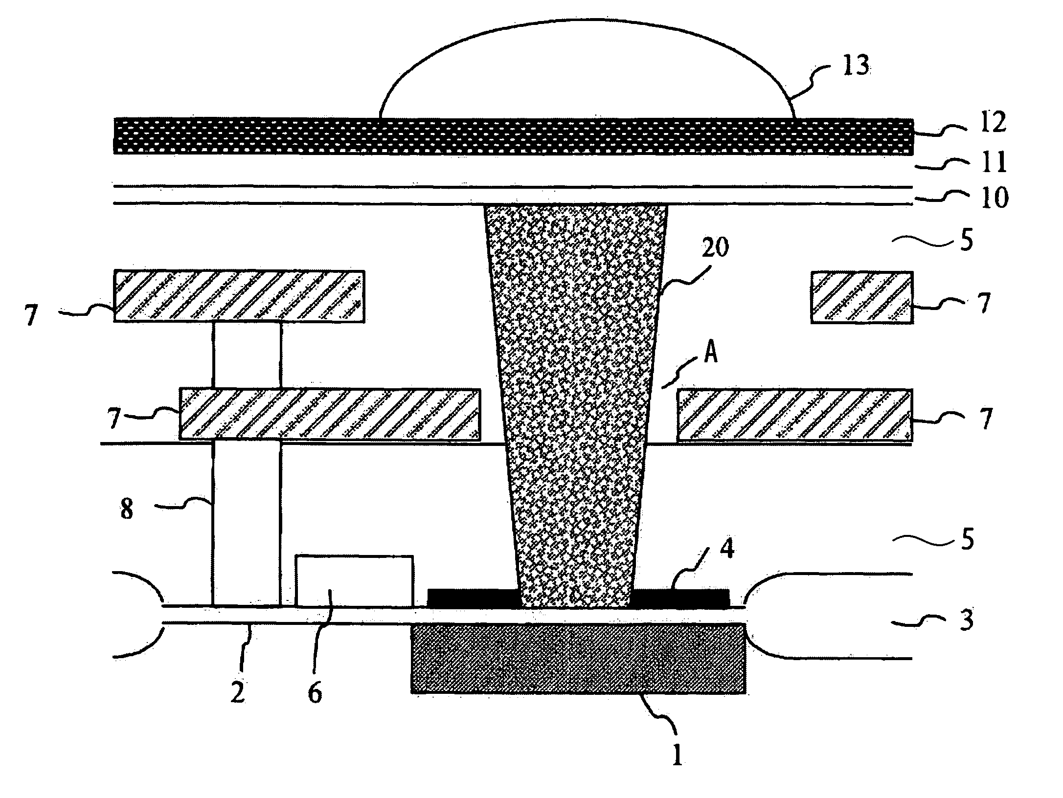
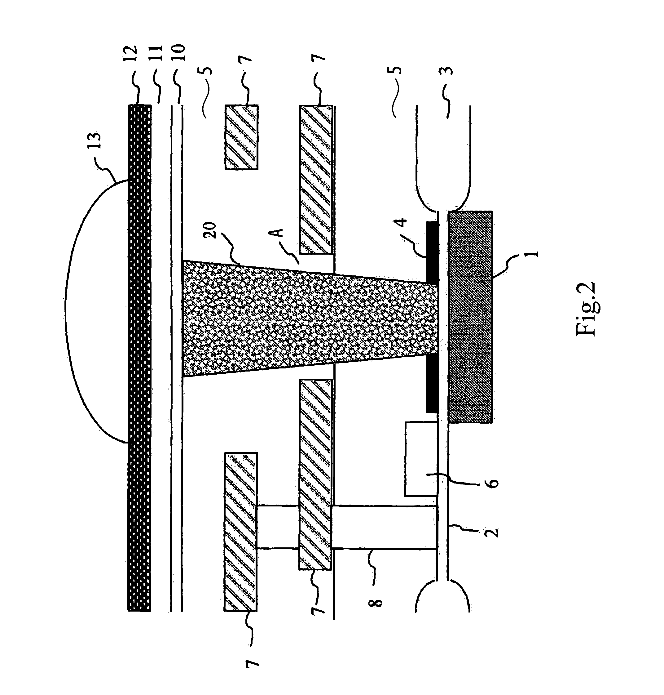
[0045] First, a general structure of a solid-state imaging device according to the present invention will be described. FIG. 2 is a sectional side elevation schematically showing an example of a structure of a solid-state imaging device according to a first embodiment (hereinafter referred to as “Embodiment 1”) of the present invention. In FIG. 2, the same reference numerals are used for the same elements as those of the conventional solid-state imaging device (refer to FIG. 27).

[0046] As shown in FIG. 2, in the solid-state imaging device in this embodiment, an insulating film 5 is disposed on a substrate provided with a light-receiving section 1, which functions as a photodiode, with a gate-insulating film 2, an element isolation insulating film 3, and a stopper SiN film (etch stopper film) 4 therebetween. The insulating film 5 is embedded with a read gate 6 which is required to read signal charges from the light-receiving section 1, a multi-layered signal lines 7, and conductive ...

embodiment 2

[0079] Next, a method for fabricating a solid-state imaging device according to a second embodiment (hereinafter referred to as “Embodiment 2”) of the present invention will be described. FIGS. 13A to 13K are sectional side elevations illustrating a method for fabricating a solid-state imaging device according to Embodiment 2 of the present invention. In order to facilitate the description, the configurations of the element region, element isolation region, etc., provided on the silicon substrate as a base are not shown in the drawings.

[0080] In Embodiment 2, as shown in FIG. 13A, a silicon substrate 111 is provided with a diode 112 which performs photoelectric conversion, a SiN film 113, a poly-interlayer film 114, first signal lines 116, an interlayer film 115 for the first signal lines, a diffusion prevention film 121 composed of copper (Cu) applied to the first wiring, an interlayer film 122 between the first signal lines and second signal lines, second signal lines 123, a diff...

embodiment 3

[0089] Next, a method for fabricating a solid-state imaging device according to a third embodiment (hereinafter referred to as “Embodiment 3”) of the present invention will be described. FIGS. 14A to 14K are sectional side elevations illustrating a method for fabricating a solid-state imaging device according to Embodiment 3 of the present invention. Here, in order to facilitate the description, the configurations of the element region, element isolation region, etc., provided on the silicon substrate as a base are not also shown in the drawings.

[0090] In Embodiment 3, a silicon substrate 211 is provided with a diode 212 which performs photoelectric conversion, a SiN film 213, a poly-interlayer film 214, first signal lines 216, an interlayer film 215 between the first signal lines, a diffusion prevention film 221 composed of Cu applied to the first wiring, an interlayer film 222 between the first signal lines and second signal lines, second signal lines 223, a diffusion prevention ...


PUM


Abstract

By improving the embedding property of a light-transmissive material constituting a waveguide, light collection efficiency is improved, and reliability of a solid-state imaging device is ensured.
In a solid-state imaging device including a light-receiving section (1) which performs photoelectric conversion in response to receipt of light and a waveguide (20) composed of a light-transmissive material formed in an insulating film 5 which covers a substrate provided with the light-receiving section (1), in which the waveguide (20) guides incident light from outside to the light-receiving section (1), the waveguide (20) is provided with a forward tapered portion in which the size of the planar shape viewed from the direction of incident light decreases from the light incident side surface toward the light-receiving section.

Description

TECHNICAL FIELD [0001] The present invention relates to a solid-state imaging device having a waveguide structure and a method for fabricating the solid-state imaging device. BACKGROUND ART [0002] MOS sensors are solid-state imaging devices which have recently been actively developed as a result of reviewing their features, such as lower power consumption than CCD sensors. In such MOS sensors, unlike CCD sensors, charges stored in light-receiving sections are not read from imaging regions by reading the insides of substrates, but charges stored are read out as electric (voltage) signals to signal lines, in the vicinity of light-receiving sections, and output from the imaging regions through the signal lines. The signal lines are referred to as output signal lines and are disposed above the substrates. Besides the output signal lines, signal lines for supplying signals to read electrodes in order to initially read out the charges stored in the light-receiving sections and reset signa...

Claims


Application Information

Patent Timeline
IPC IPC(8): G02B6/10H01L27/146H04N5/225
CPCH01L27/14601H01L27/14623H04N5/2254H01L27/14629H01L27/14627H01L27/146
Inventor KOMOGUCHI, TETSUYAENOMOTO, YOSHIYUKI
Owner SONY CORP
Why Eureka
Try Eureka