Cleaning with electrically charged aerosols

an aerosol and electrical charge technology, applied in the direction of cleaning process and equipment, cleaning liquids, chemistry apparatus and processes, etc., can solve the problems of not being able to overcome the primary adhesion force which must be overcome to remove contaminant particles, easy to be damaged or destroyed by even tiny particles of dust or metal, and applying too much electrical charge, etc., to achieve the effect of improving cleaning performan

Inactive Publication Date: 2006-06-08
SEMITOOL INC
View PDF8 Cites 44 Cited by
  • Summary
  • Abstract
  • Description
  • Claims
  • Application Information

AI Technical Summary

Benefits of technology

[0008] A new cleaning technology with major advantages has now been developed. In a first aspect of the invention, in a method for cleaning a workpiece, the workpiece is placed into a processing chamber. An electrically charged aerosol of liquid droplets is formed by an aerosol generator. The aerosol generator may be in the chamber, or outside of the chamber, with the aerosol then moved into the chamber. The electrically charged aerosol droplets are directed to or conveyed to the workpiece. This creates an electrical charge on the workpiece. The electrical charge repels contaminant particles from the surface of the workpiece. A liquid film is advantageously maintained on the workpiece surface. Contaminant particles repelled from the workpiece surface are entrained in and carried away by the liquid film. Cleaning performance is improved.

Problems solved by technology

Since the devices are microscopic, they can very easily be damaged or destroyed by even tiny particles of dust or metal, or from residue of process liquids or vapors, fingerprints, etc.
The cleaning techniques used in the past that focus solely on chemical and physical methods, may therefore fail to counteract the primary adhesion forces which must be overcome to remove contaminant particles.
Applying too much of an electrical charge can damage or destroy semiconductor devices.
Consequently, obtaining improved cleaning performance presents difficult engineering challenges.

Method used


Image

  • Cleaning with electrically charged aerosols
  • Cleaning with electrically charged aerosols
  • Cleaning with electrically charged aerosols

Examples


Embodiment Construction

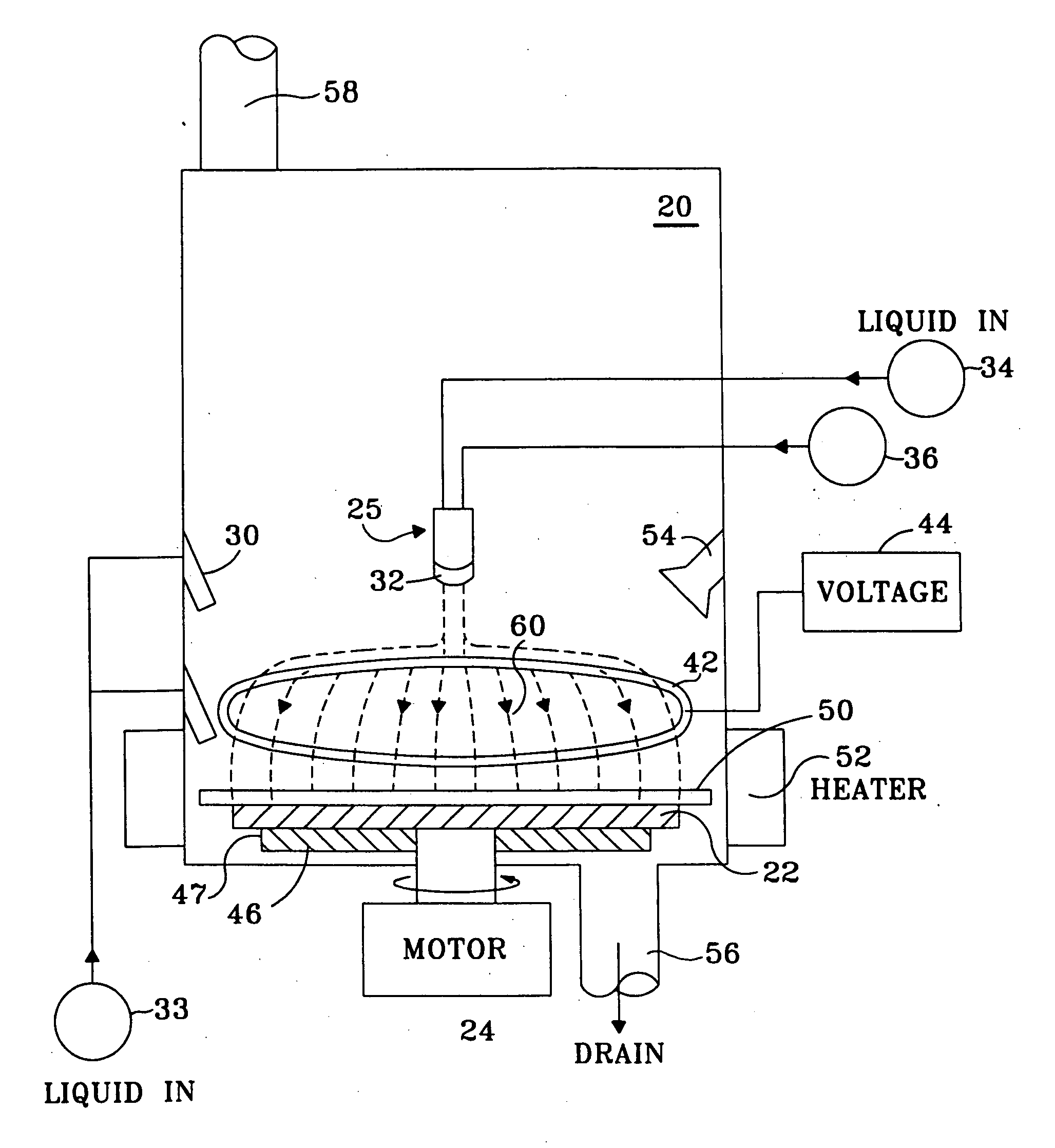
[0018] The systems and methods described here may be used to treat workpieces such as semiconductor wafers, flat panel displays, hard disk media, CD glass, memory and optical media, MEMS devices, and various other substrates on which micro-electronic, micro-mechanical, or micro-electromechanical devices are or can be formed. These are collectively referred to here as workpieces or wafers. Descriptions here of semiconductors, or the semiconductor industry or manufacturing, also include the workpieces listed above, and their equivalents.

[0019] In a cleaning process, a workpiece is placed into a processing chamber. The wafer may be either stationary or it may be moving during the process. An electrically charged aerosol is formed by an aerosol generator. A liquid layer is provided on the workpiece. At the target cleaning or aerosol delivery area, the liquid layer is thinned or reduced down to a microscopic film. The aerosol is propelled to and / or through the liquid film at the target ...


PUM


Abstract

In a method for cleaning a wafer, the wafer is placed a processing chamber. A layer or film of liquid is provided on the wafer. Electrically charged aerosol droplets of a liquid are formed and directed to the workpiece. The charged aerosol particles accumulate on the workpiece. This creates an electrical charge on the workpiece. Contaminant particles on the workpiece are released and/or repelled by the electrical charge and are carried away in the liquid layer. The liquid layer is optionally continuously replenished with fresh liquid. The liquid layer may be thinned out in a localized aerosol impingement area, via a jet of gas, to allow the electrical charge of the aerosol to better collect on or near the surface of the workpiece.

Description

BACKGROUND OF THE INVENTION [0001] Semiconductor devices are essential in modern life. Virtually all of today's electronic products could not exist without semiconductor devices. These products include computers, cell phones and communication devices, consumer electronics, medical devices, military equipment, and many other products. Many of these electronic products are used by virtually everyone in the United States on a daily basis. [0002] Semiconductor devices are manufactured by performing many separate steps on substrates or wafers. These steps include polishing, photolithography, coating, metal plating, etching, etc. Cleaning is also very important in manufacturing semiconductor devices. Since the devices are microscopic, they can very easily be damaged or destroyed by even tiny particles of dust or metal, or from residue of process liquids or vapors, fingerprints, etc. Cleaning removes these contaminants or prevents or reduces creation of contaminants in the first place. [00...

Claims


Application Information

Patent Timeline
Patent Type & Authority Applications(United States)
IPC IPC(8): B08B3/12B08B3/00
CPCB08B3/02B08B3/10H01L21/02052H01L21/67051B08B3/12B08B2203/0288
Inventor BERGMAN, ERIC J.SCRANTON, DANA R.AEGERTER, BRIAN
Owner SEMITOOL INC
Why Eureka
Try Eureka