CMOS device with selectively formed and backfilled semiconductor substrate areas to improve device performance

a technology of semiconductor substrate and semiconductor device, applied in the field of mosfet device formation, can solve the problems of reducing affecting the performance of nmos device, and limited success of approaches

Inactive Publication Date: 2006-06-08
TAIWAN SEMICON MFG CO LTD
View PDF6 Cites 38 Cited by
  • Summary
  • Abstract
  • Description
  • Claims
  • Application Information

AI Technical Summary

Problems solved by technology

These approaches have met with limited success, however, since the formation of particular type of stress (strain), for example compressive or tensile stress in a channel region of one type of majority charge carrier device, for example a PMOS device, will tend to have a degrading effect on a device of the opposite majority charge carrier, e.g., an NMOS device.
For example, introducing compressive strain into a device channel region will tend to improve PMOS device performance but degrade NMOS device performance.
While these approaches have been shown to be successful, the degrading effect on a device of opposite polarity in dual gate CMOS structures is difficult to overcome, typically requiring a complex series of processing steps.
In addition, subsequent manufacturing processes including thermal cycling of the channel region may operate to relax the induced stress (strain) over time, thereby leading to instability and unreliability in device performance.

Method used


Image

  • CMOS device with selectively formed and backfilled semiconductor substrate areas to improve device performance
  • CMOS device with selectively formed and backfilled semiconductor substrate areas to improve device performance
  • CMOS device with selectively formed and backfilled semiconductor substrate areas to improve device performance

Examples


first embodiment

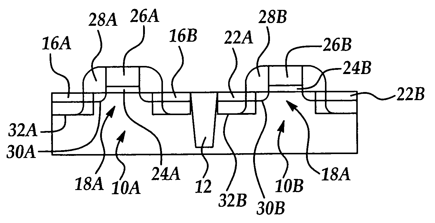
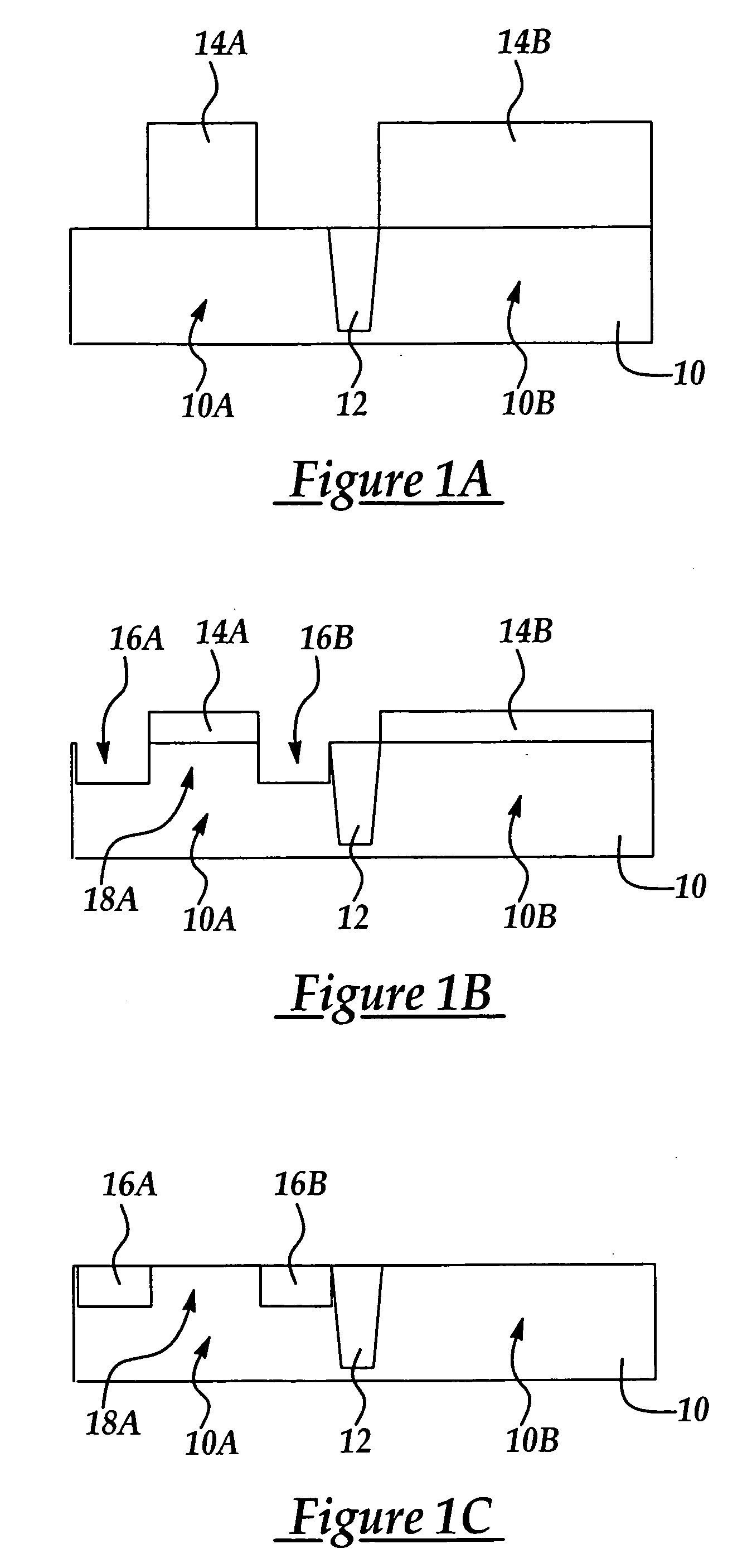
[0020] In the first embodiment as shown in FIGS. 1A-1E, when different semiconductor alloys are used to backfill the respectively formed PMOS and NMOS recessed areas having respectively expanded lattice parameters and contracted lattice parameters compared to silicon as explained further below, a recessed depth of up to about 800 Angstroms, more preferably from about 200 to about 400 Angstroms is sufficient to form the desired respective compressive and tensile stresses in the respective channel regions of the PMOS and NMOS devices.

[0021] Referring to FIG. 1C, following removal of remaining portion of the resist layer e.g., 14A and 14B portions, a semiconductor alloy comprising silicon and an element having a larger atomic radius is formed to form a first strained silicon composite (alloy), preferably semiconducting, having an expanded lattice cell volume (dimension) compared to silicon is then formed to backfill the first recessed areas 16A and 16B. In a preferred embodiment, the f...

second embodiment

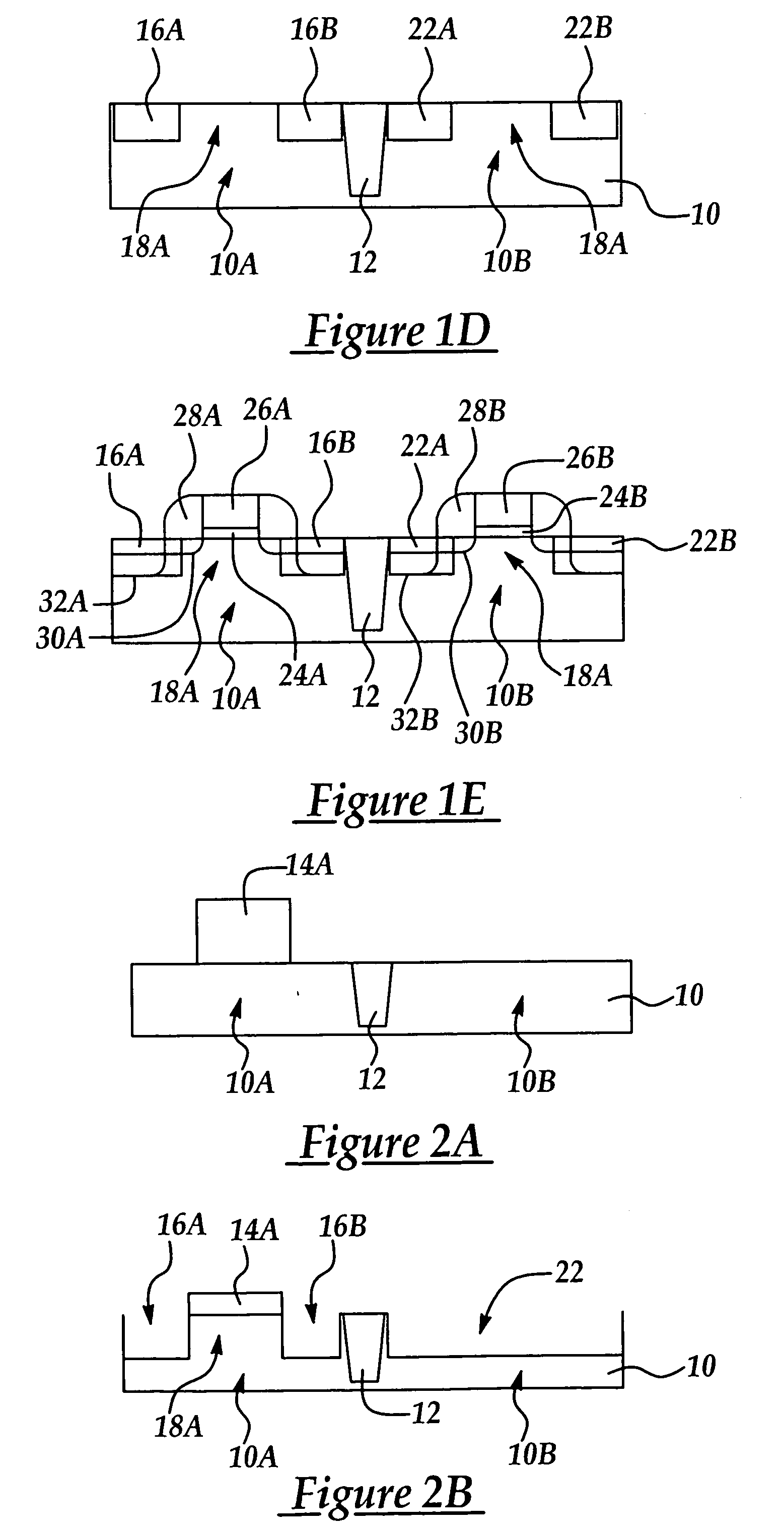
[0025] Referring to FIG. 2A, in a second embodiment according to an exemplary process flow, the silicon substrate 10 is for example phosphorous doped and the PMOS region 10A is patterned as previously outlined in FIG. 1A with resist layer portion 14A, however, in this embodiment, the NMOS substrate portion 10B is left exposed.

[0026] Referring to FIG. 2B, in a conventional wet or dry etching process, preferably a dry etching process, recessed area portions 16A and 16B are formed as previously outlines in FIG. 1B, however, the NMOS substrate portion 10B is now etched to include the channel region 18B, for example substantially the entire portion of active NMOS region 10B is etched to form a recessed portion 22. In this embodiment, the depth of the recessed area is preferably up to about 800 Angstroms, more preferably having a depth from about 200 to about 600 Angstroms.

[0027] Referring to FIG. 2C, following removal of remaining resist layer portions e.g., 14A, a semiconductor alloy c...


PUM


Abstract

An NMOS and PMOS device pair having a selected stress level and type exerted on a respective channel region and method for forming the same, the method including providing a semiconductor substrate; forming isolation regions to separate active areas comprising a PMOS device region and an NMOS device region; lithographically patterning the semiconductor substrate and etching respective recessed areas including the respective NMOS and PMOS device regions into the silicon semiconductor substrate to a predetermined depth; backfilling the respective recessed areas with at least one semiconductor alloy; and, forming gate structures and offset spacers over the respective NMOS and PMOS device regions.

Description

FIELD OF THE INVENTION [0001] This invention generally relates to formation of MOSFET devices in integrated circuit manufacturing processes and more particularly to a CMOS device and method of forming the same including selectively formed and backfilled recessed semiconductor substrate active area portions to introduce a stress type and level into a channel region of the CMOS device to improve device performance including charge carrier mobility and drive current saturation (IDsat) BACKGROUND OF THE INVENTION [0002] Mechanical stresses are known to play a role in charge carrier mobility which affects Voltage threshold (VT) shifts, drive current saturation (IDsat), and ON / Off current, all critical parameters for efficient and reliable CMOS device operation. The effect of induced mechanical stresses to strain a MOSFET device channel region, and the effect on charge carrier mobility is believed to be influenced by complex physical processes related to acoustic and optical phonon scatte...

Claims


Application Information

Patent Timeline
Patent Type & Authority Applications(United States)
IPC IPC(8): H01L29/94H01L21/8238
CPCH01L21/823807H01L21/823814H01L29/165H01L29/6659H01L29/66628H01L29/66636H01L29/7833H01L29/7848
Inventor HUANG, YI-CHUNTAO, HUN-JANLIN, CHUN-CHIEHKO, CHIH-HSIN
Owner TAIWAN SEMICON MFG CO LTD
Why Eureka
Try Eureka