Supercharge Your Innovation With Domain-Expert AI Agents!

Mask and method for crystallizing amorphous silicon

a crystallization method and crystallization method technology, applied in the field of crystallization methods, can solve the problems of reducing the reliability of thin film transistors, non-uniform grains, and non-compliance with the size of grains, so as to reduce the number of processes

Inactive Publication Date: 2006-06-08
LG DISPLAY CO LTD
View PDF4 Cites 9 Cited by
  • Summary
  • Abstract
  • Description
  • Claims
  • Application Information

AI Technical Summary

Benefits of technology

The present invention provides a mask and method for crystallizing amorphous silicon to form polycrystalline silicon with large grains. The mask includes a base substrate, a phase shift layer, and a blocking layer, and the method involves placing the mask over the substrate and applying a laser beam onto the amorphous silicon layer through the mask. The technical effects of the invention include improved quality of polycrystalline silicon with large grains, reduced number of processes, and improved efficiency.

Problems solved by technology

However, the quartz substrate may not be cost effective for a substrate of thin film transistors.
However, sizes of the grains are non-uniform.
Generally, grain boundaries of polycrystalline silicon interfere with currents and lowers the reliability of a thin film transistor.
In addition, a breakdown of an insulating layer may occur because of a collision of electrons and a deterioration in the grains.
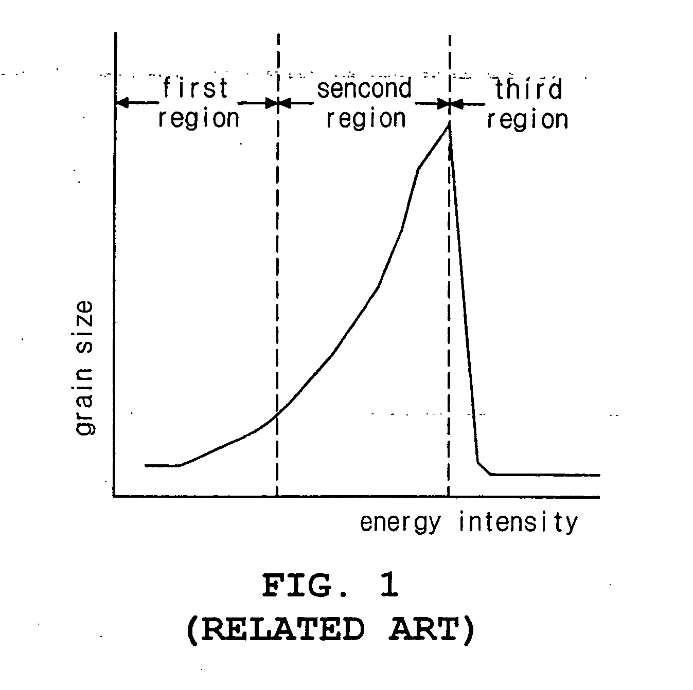
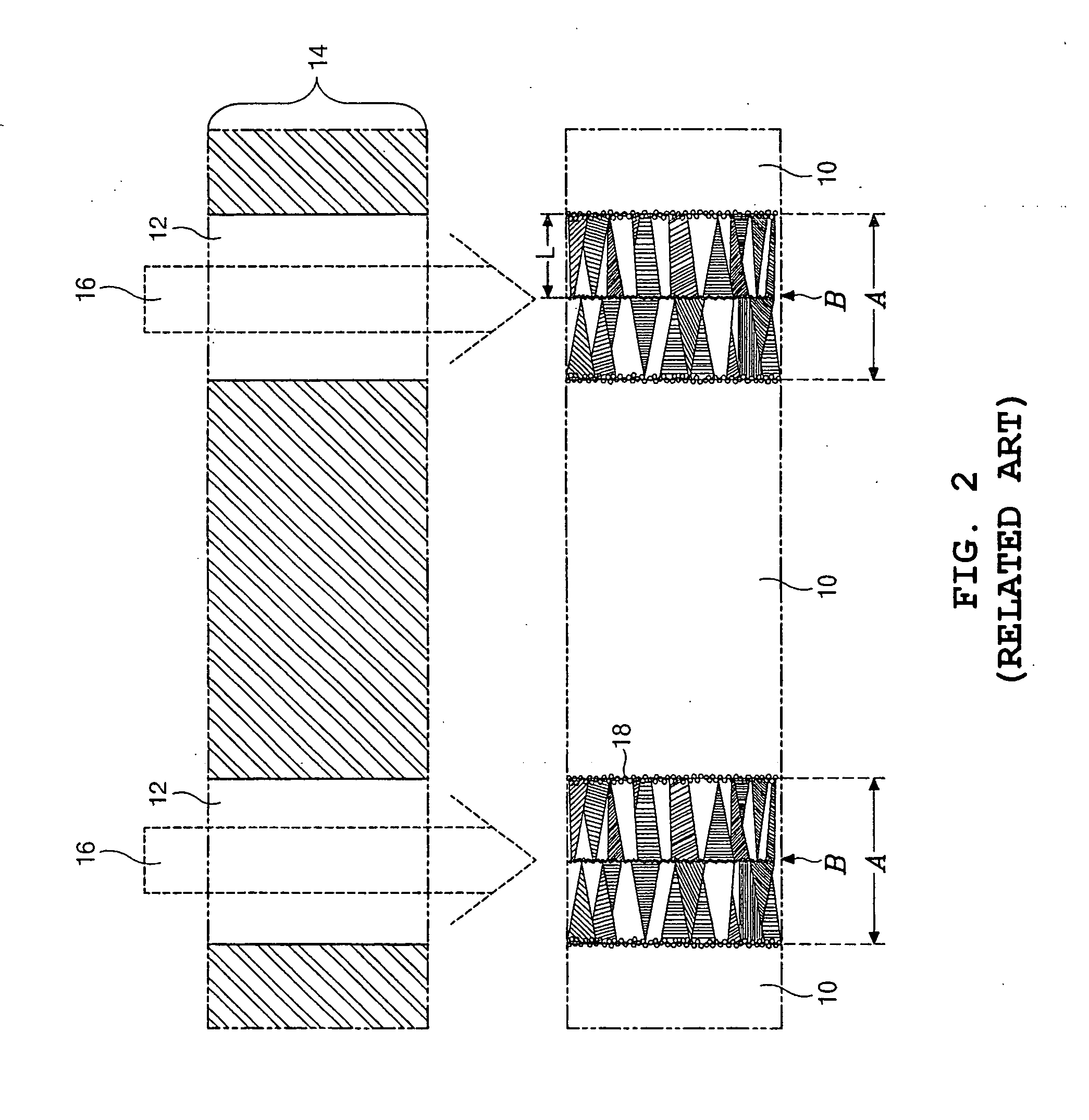
More particularly, in the SLS crystallizing process using the mask of the related art, if the peaks of a laser shot overlap each other, the silicon layer is melted non-uniformly because an overlapping portion between the peaks is large, and thus the grains do not grow completely.
In addition, since a nucleation region is formed in the overlapping portion, characteristics of crystallization get worse.
However, there is a disadvantage in that the efficiency of the process is lowered due to an increase in the laser shots.

Method used


Image

  • Mask and method for crystallizing amorphous silicon
  • Mask and method for crystallizing amorphous silicon
  • Mask and method for crystallizing amorphous silicon

Examples


Embodiment Construction

[0048] Reference will now be made in detail to the preferred embodiments of the present invention, examples of which are illustrated in the accompanying drawings. Wherever possible, the same reference numbers will be used throughout the drawings to refer to the same or like parts.

[0049]FIG. 5 is a schematic view illustrating the principle of phase shift in a mask according to the present invention.

[0050] In FIG. 5, a first part 54a of a laser beam 54 passes through a first portion M1 of a mask 50, where there is no layer, and a second part 54b of the laser beam 54 permeates a second portion M2 of the mask 50, where there exists a phase shift layer 52. Since the first part 54a and the second part 54b of the laser beam 54 go through different optical paths according to the existence of the phase shift layer 52, there is a phase difference ΔΦ between the first part 54a and the second part 54b passing through the mask 50. The phase difference ΔΦ is expressed as the following equation:...


PUM

PropertyMeasurementUnit
widthaaaaaaaaaa
widthaaaaaaaaaa
transition temperatureaaaaaaaaaa

Abstract

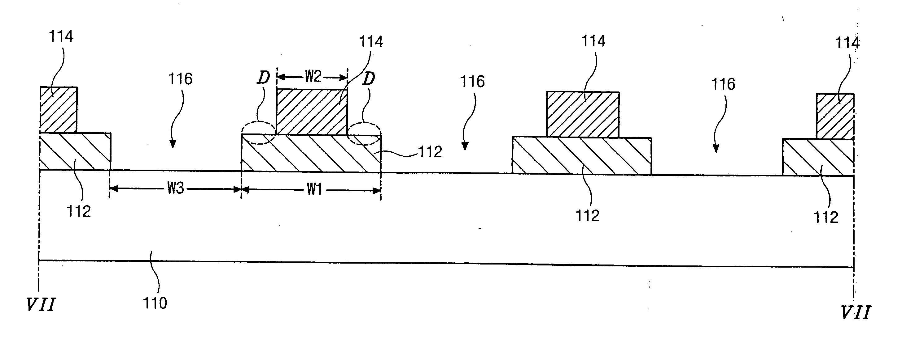
A method of crystallizing amorphous silicon includes forming an amorphous silicon layer on a substrate, placing a mask over the substrate including the amorphous silicon layer, and applying a laser beam onto the amorphous silicon layer through the mask to form a first crystallized region, the laser beam having an energy intensity high enough to completely melt the amorphous silicon layer, wherein the mask comprises a base substrate, a phase shift layer on the base substrate, having a plurality of first stripes having a first width separated by slits, and a blocking layer overlapping the phase shift layer, having a plurality of second stripes having a second width narrower than the first width, the second stripes being parallel to the first stripes.

Description

[0001] This application claims the benefit of the Korean Patent Application No. P2002-060705 filed on Oct. 4, 2002, which is hereby incorporated by reference. BACKGROUND OF THE INVENTION [0002] 1. Field of the Invention [0003] The present invention relates to a crystallizing method, and more particularly, to a mask and method for crystallizing amorphous silicon. Although the present invention is suitable for a wide scope of applications, it is particularly suitable for improving fabrication productivity. [0004] 2. Discussion of the Related Art [0005] A liquid crystal display (LCD) device has been in the spotlight as a next generation high value display device because of its low power consumption and portability. [0006] The liquid crystal display device is composed of an array substrate including thin film transistors, a color filter substrate, and a liquid crystal layer interposed between an array substrate and a color filter substrate. The liquid crystal display device displays ima...

Claims


Application Information

Patent Timeline
Patent Type & Authority Applications(United States)
IPC IPC(8): C30B15/30C30B15/26C30B11/00G03F1/00G02F1/13C30B13/24C30B29/06G03F1/08H01L21/20H01L21/336H01L21/77H01L21/84H01L29/786
CPCC30B13/24Y10T117/10G03F1/08G03F1/26G03F1/29G03F1/32H01L21/02532H01L21/0268H01L21/02686H01L29/6675H01L29/78672H01L29/78696H01L27/1281H01L27/1285Y10T117/1008Y10T117/1004C30B29/06G02F1/13
Inventor HWANG, KWANG-JO
Owner LG DISPLAY CO LTD
Features
  • R&D
  • Intellectual Property
  • Life Sciences
  • Materials
  • Tech Scout
  • Unparalleled Data Quality
  • Higher Quality Content
  • 60% Fewer Hallucinations
Learn More