

Liquid crystal display device and fabricating method thereof
- Summary
- Abstract
- Description
- Claims
- Application Information
AI Technical Summary
Benefits of technology
Problems solved by technology
Method used
Image

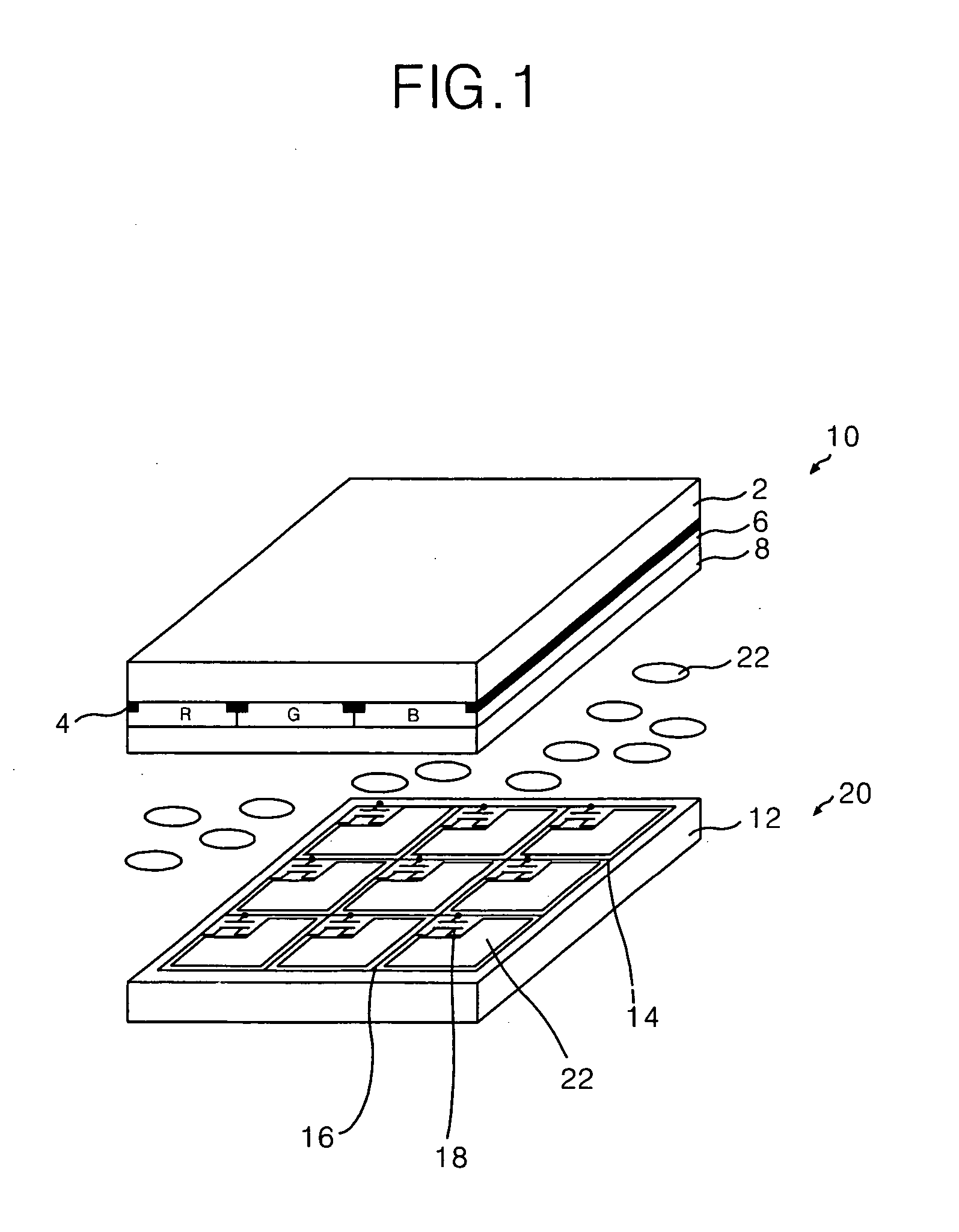
Examples
first embodiment
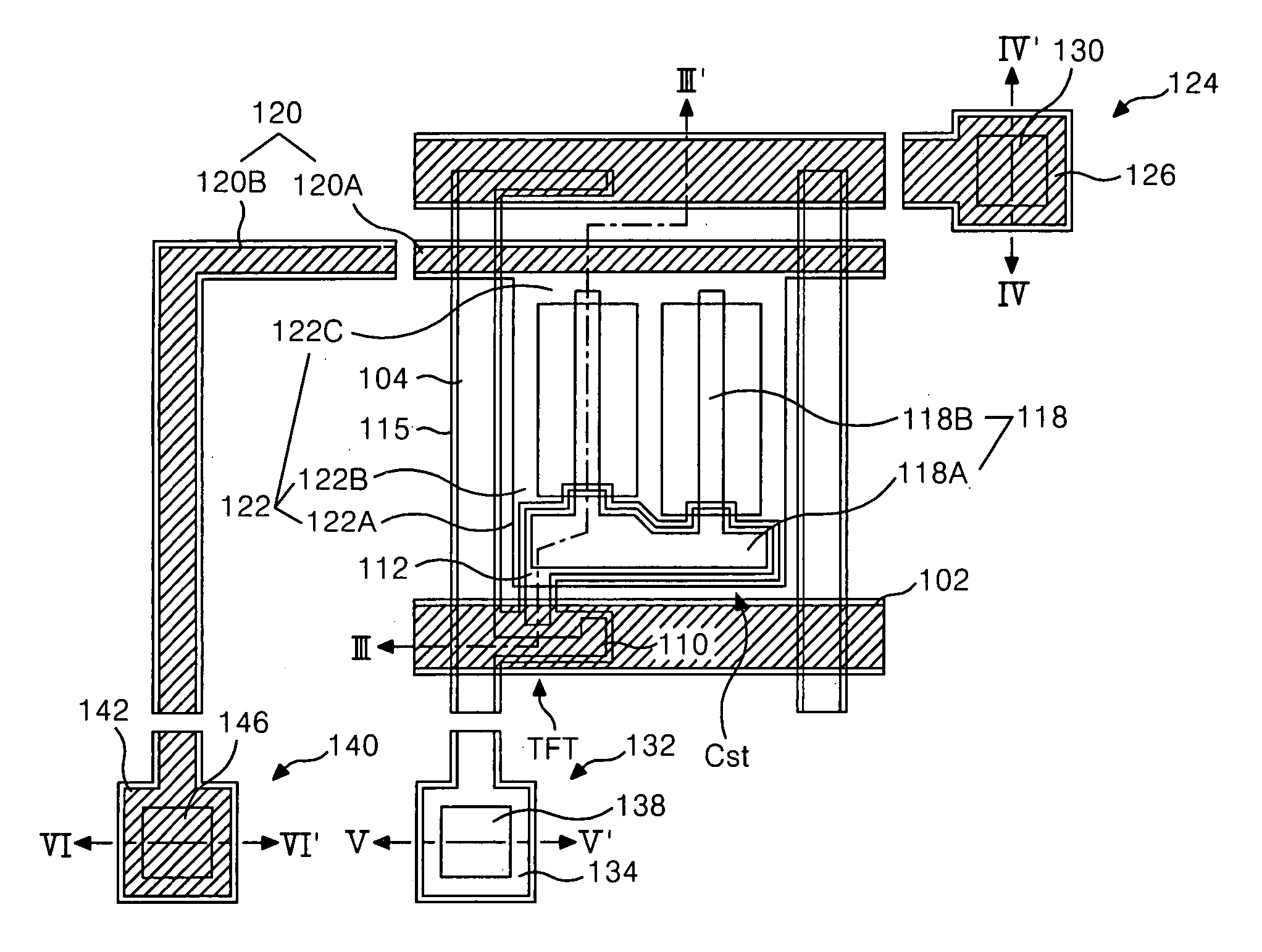
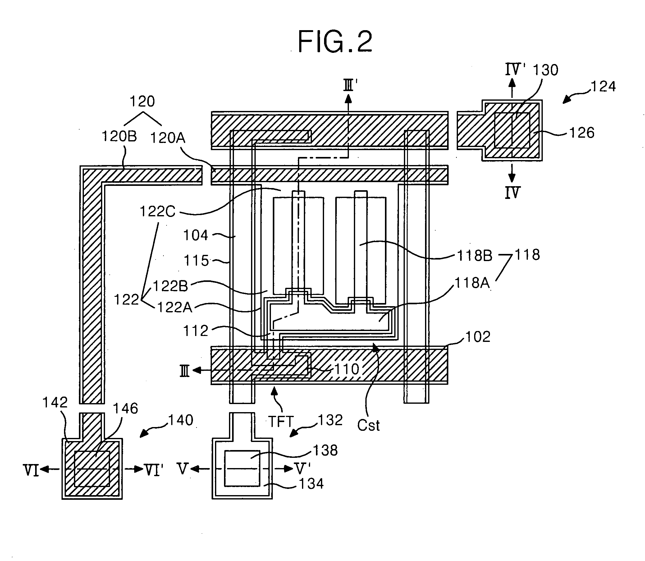
[0042]FIG. 2 is a plan view illustrating a structure of a thin film transistor substrate of horizontal electric field applying type according to the present invention, and FIG. 3 is a sectional views of the thin film transistor substrate taken along the III-III′, IV-IV′, V-V′, and VI-VI′lines in FIG. 2.
[0043] Referring to FIG. 2 and FIG. 3, the thin film transistor substrate of horizontal electric field applying type includes a gate line 102 and a data line 104 provided on a lower substrate 150 in such a manner to intersect each other with having a gate insulating film 152 therebetween and define a pixel area, a thin film transistor TFT connected to the gate line 102, the data line 104, a pixel electrode 118, a pixel electrode 118 and a common electrode 122 provided to form a horizontal electric field at said pixel area, and a common line 120 connected to the common electrode 122. Further, the thin film transistor substrate includes a storage capacitor Cst provided at an overlapping...
second embodiment
[0085]FIG. 11 is a plan view illustrating a portion of a thin film transistor substrate according to the present invention, and FIG. 12 is a section view of the thin film transistor substrate taken along the IV-IV′, V-V′, VI-VI′, and VII-VII′ lines in FIG. 11.
[0086] The gate line 202 and the data line 204 cross each other with having a gate insulating film 252 therebetween to define the pixel area. Herein, the gate line 202 has a double-layer structure in which a first conductive layer 201 formed of a transparent conductive layer and a second conductive layer 203 formed of an opaque metal are built.
[0087] The thin film transistor TFT includes a gate electrode included in the gate line 202, a source electrode 210 connected to the data line 204, a drain electrode 212 positioned in opposition to the source electrode 210 to be connected to a pixel electrode 218, an active layer 214 overlapping with the gate line 202 with the gate insulating film 252 therebetween to provide a channel be...
PUM
 Abstract
Description
Claims
Application Information