Semiconductor device and method for manufacturing the same

a technology of semiconductors and semiconductors, applied in the direction of semiconductor devices, electrical devices, transistors, etc., can solve the problems of reducing the characteristics of transistors in some cases, excessive diffusion of impurities, and prone to problems particularly

Inactive Publication Date: 2006-06-08
FUJITSU LTD
View PDF5 Cites 7 Cited by
  • Summary
  • Abstract
  • Description
  • Claims
  • Application Information

AI Technical Summary

Benefits of technology

[0017] In view of the foregoing, it is an object of the present invention to provide a method for manufacturing a high-performance and high-quality semiconductor device comprising a gate electrode, and a sidewall provided on the gate electrode, and to provide the semiconductor device.

Problems solved by technology

However, when the film formation is performed under the high temperature conditions, the following problem arises.
For example, impurities introduced into the gate electrode or the semiconductor substrate prior to the film formation are excessively diffused, which leads to reduction in transistor characteristics in some cases.
However, when using the film as a sidewall, the following problems remain.
For example, when using the silicon nitride film for the whole part or a part of the sidewall, the following problems are caused irrespective of the film formation method.
Further, since the silicon nitride film is usually formed under higher temperature conditions as compared with the silicon oxide film, impurities are excessively diffused.
However, also when using the silicon oxide film for the sidewall, the following problems are caused.
When a metal such as cobalt (Co) used in the silicification remains even in a small amount on the sidewall 103 surface, the problem readily occurs particularly.
In this case, however, the problem of impurity diffusion as described above may occur, which is likely to cause reduction in transistor characteristics.

Method used


Image

  • Semiconductor device and method for manufacturing the same
  • Semiconductor device and method for manufacturing the same
  • Semiconductor device and method for manufacturing the same

Examples


Embodiment Construction

[0060] Preferred embodiments of the present invention will be described below with reference to the accompanying drawings, wherein like reference numerals refer to like elements throughout.

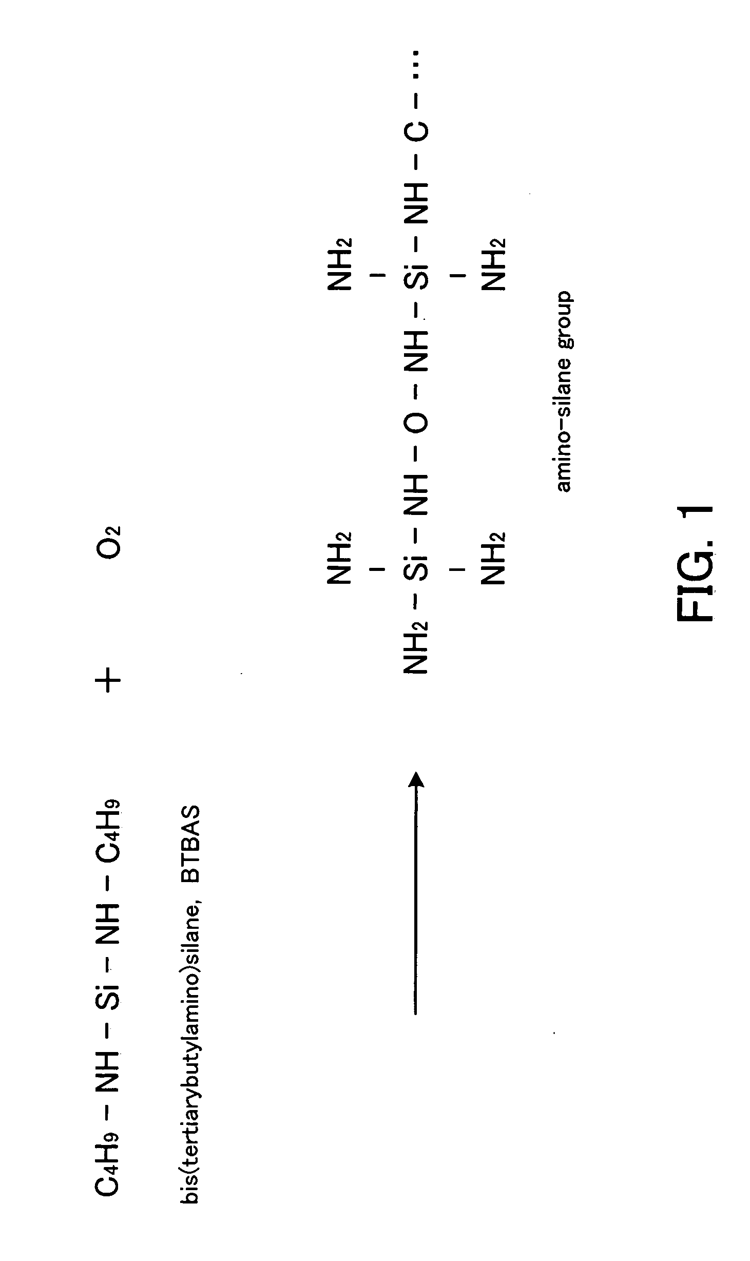
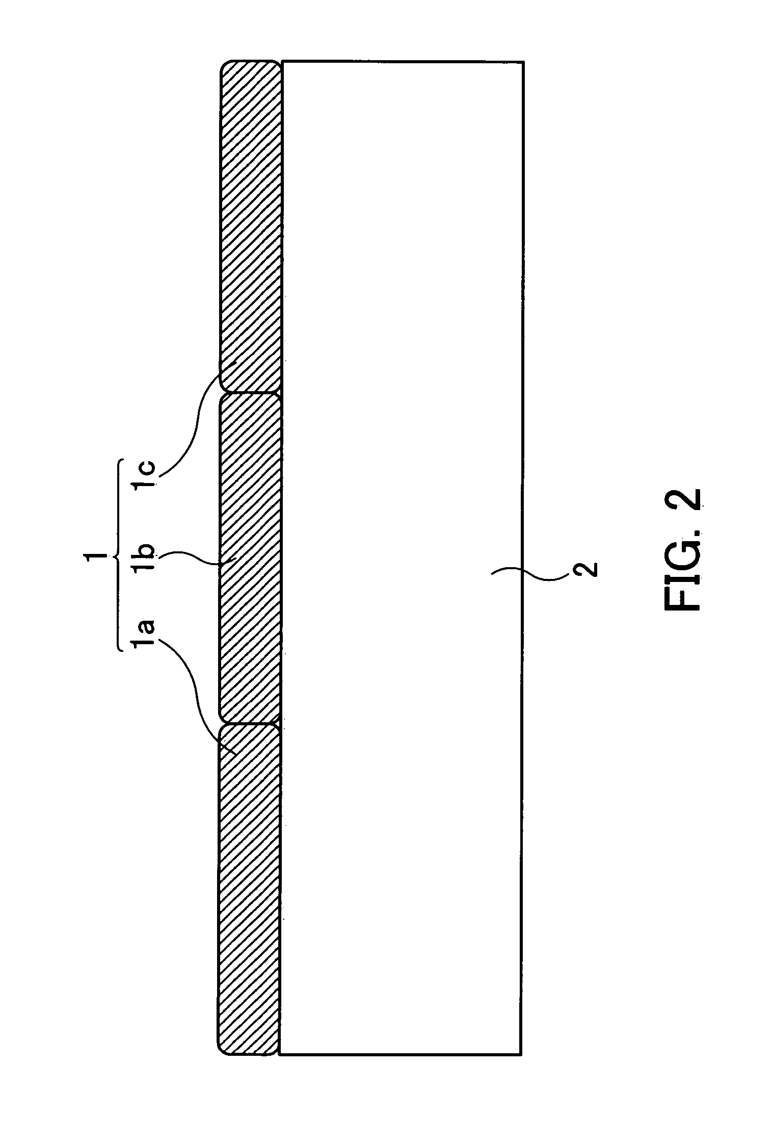
[0061]FIG. 1 shows a film formation mechanism of a carbon-containing silicon nitride oxide film. FIG. 2 is a schematic cross-sectional view showing a part of a carbon-containing silicon nitride oxide film formed on a semiconductor substrate.

[0062] As shown in FIG. 1, the carbon-containing silicon nitride oxide film can be formed using BTBAS and oxygen (O2) as starting materials by a thermal CVD method under the following conditions. The pressure within the film formation room is set to about 0.1 to about 1000 Pa, preferably about 5 to about 100 Pa. The film formation temperature is set to low temperature conditions of about 300 to about 650° C., preferably about 450 to about 580° C. The film formation time is set according to the pressure within the film formation room or the film formation temp...


PUM

PropertyMeasurementUnit
temperatureaaaaaaaaaa
pressureaaaaaaaaaa

Abstract

Disclosed is a method for manufacturing a semiconductor device provided with a sidewall having a high quality and an excellent shape. The sidewall on a gate electrode side wall is formed using a carbon-containing silicon nitride oxide film. The film can be formed by a CVD method using, as starting materials, BTBAS and oxygen where a BTBAS flow rate/oxygen flow rate ratio is appropriately set and a low film formation temperature is set, for example, at about 530° C. When forming the sidewall using this film, improvement in HF resistance and reduction in fringe capacitance can be realized due to contribution of nitrogen atoms and carbon atoms. Further, when forming this film under low temperature conditions, unnecessary diffusion of impurities introduced into a semiconductor substrate can be suppressed. Thus, transistor characteristics are enhanced and stabilized, so that high performance and high quality in the semiconductor device can be realized.

Description

CROSS-REFERENCE TO RELATED APPLICATIONS [0001] This application is based upon and claims the benefits of priority from the prior Japanese Patent Application No. 2004-350749, filed on Dec. 3, 2004, the entire contents of which are incorporated herein by reference. BACKGROUND OF THE INVENTION [0002] 1. Field of the Invention [0003] The present invention relates to a semiconductor device and a method for manufacturing the same. More particularly, the present invention relates to a semiconductor device comprising a gate electrode and a sidewall provided on the gate electrode. The invention also pertains to a method for manufacturing the same. [0004] 2. Description of the Related Art [0005] In a semiconductor device, a sidewall is provided on a side wall of a gate electrode, and plays the roll of electrically separating a gate electrode and an impurity region within a transistor. The gate electrode is formed on a semiconductor substrate such as a silicon substrate. The impurity region su...

Claims


Application Information

Patent Timeline
Patent Type & Authority Applications(United States)
IPC IPC(8): H01L21/3205
CPCH01L21/28518H01L21/3145H01L21/76837H01L21/76895H01L21/823814H01L21/823864H01L29/665H01L29/6653H01L29/6656H01L29/6659H01L29/7833H01L21/02115H01L21/02271H01L21/02211H01L21/0217
Inventor OHTA, HIROYUKIOOKOSHI, KATSUAKIMORI, TOSHIFUMI
Owner FUJITSU LTD
Why Eureka
Try Eureka