Contact resistance reduction by new barrier stack process

a technology of contact resistance and barrier stack, which is applied in the direction of semiconductor/solid-state device manufacturing, basic electric elements, electric devices, etc., can solve the problems of reducing device reliability, reducing the ability to deposit continuous films, and reducing the reentrant profile, so as to reduce the reentrant profile

Active Publication Date: 2006-06-08
TEXAS INSTR INC
View PDF66 Cites 186 Cited by
  • Summary
  • Abstract
  • Description
  • Claims
  • Application Information

AI Technical Summary

Benefits of technology

[0011] To address the above-discussed deficiencies of the prior art, the present invention provides a method for forming an interconnect, an interconnect using the method, a method for forming an integrated circuit using the method, and another method for forming an interconnect. In one embodiment, the method of forming an interconnect includes forming an open...

Problems solved by technology

High quality contacts are essential to high device yield and reliability, but fabrication of these high quality contacts poses several technical challenges.
These constraints lead to contacts with aspect ratios large enough to present manufacturing challenges.
One such challenge is removing contaminants from the bottom of the contact hole before depositing one or more barrier layers into the hole.
Contamination has the effect of increasing the contact resistance, Rc, of the contact and reducing device reliability.
To some extent, however, the PSE also knocks dielectric material off the sidewall of the contact hole, which redeposits onto the bottom of the hole.
Thus, there is a competition between removal of contamination from the bottom of the hole and redeposition of sidewall material.
Another critical challenge is the ability to deposit continuous films into the con...

Method used


Image

  • Contact resistance reduction by new barrier stack process
  • Contact resistance reduction by new barrier stack process
  • Contact resistance reduction by new barrier stack process

Examples


Embodiment Construction

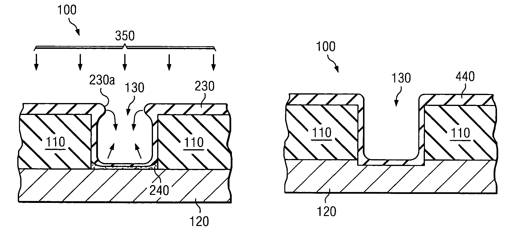
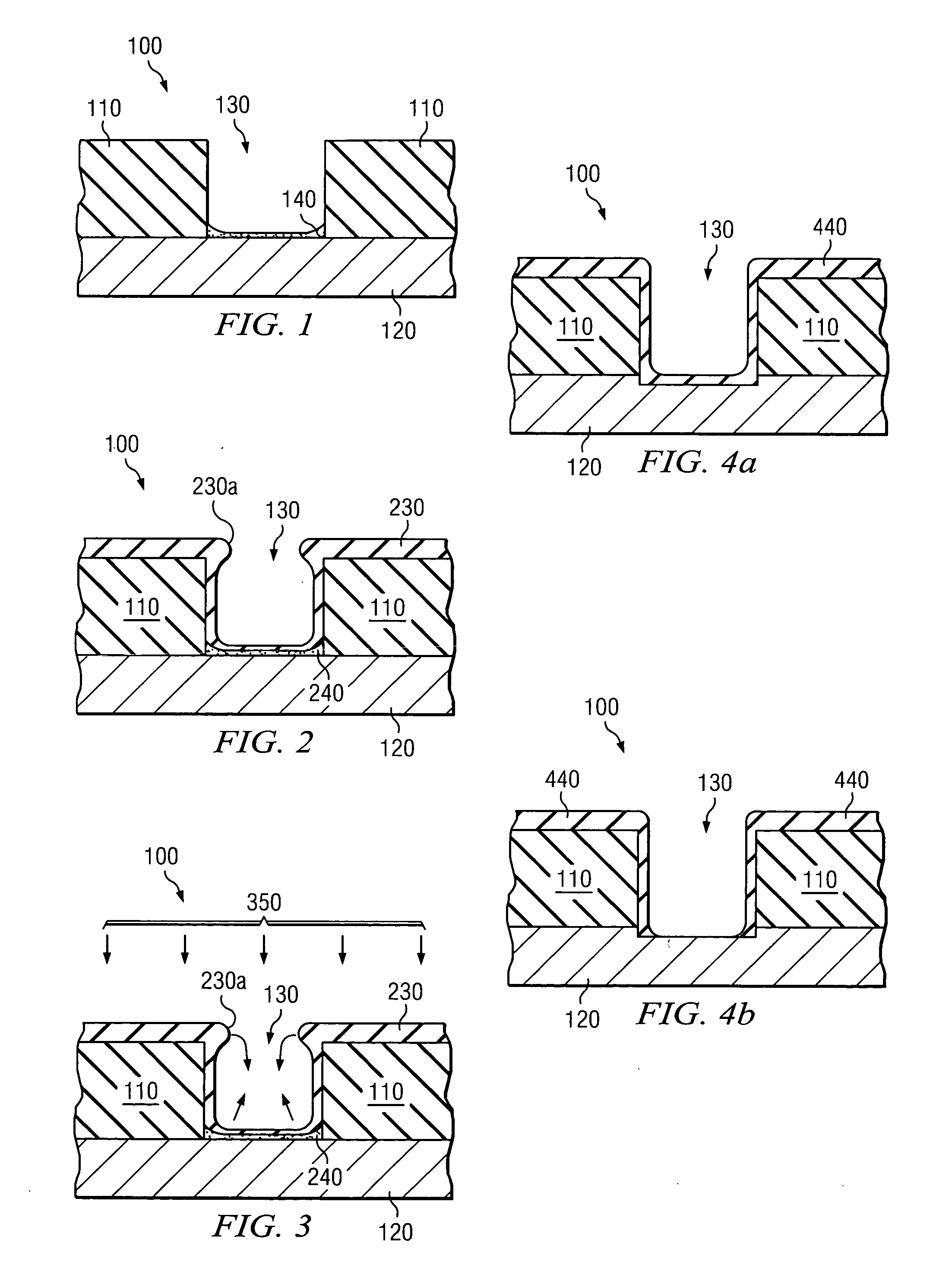
[0026] Referring initially to FIG. 1, illustrated is a sectional view of a semiconductor device 100 at an early stage of manufacture. A dielectric layer 110 overlies conductive layer 120. Dielectric layer 110 may be a conventional dielectric used to space the semiconductor devices from the first interconnect level, such as phosphorous-doped silicon dioxide. However, the presently claimed invention is not limited to a particular dielectric and doping. Conductive layer 120 may also be formed conventionally, and further may be a metal silicide such as NiSi, though one skilled in the art will appreciate other compounds of a metal and semiconductor could also be used as the conductive layer. Opening 130 has been formed in dielectric 110 by conventional means, after which contamination 140 may be present at the bottom of the opening 130. The sidewalls of opening 130 are shown as substantially vertical. In practice, however, the sidewall may have some slope, with the width of opening 130 g...


PUM


Abstract

The present invention provides a method for forming an interconnect on a semiconductor substrate 100. The method includes forming an opening 230 over an inner surface of the opening 130, the depositing forming a reentrant profile near a top portion of the opening 130. A portion of barrier 230 is etched, which removes at least a portion of the barrier 230 to reduce the reentrant profile. The etching also removes at least a portion of the barrier 230 layer at the bottom of the opening 130.

Description

TECHNICAL FIELD OF THE INVENTION [0001] The present invention is directed, in general, to deposition of conducting films on a semiconductor substrate and, more specifically, to a method for deposition of barrier materials in contact holes to reduce the series resistance of the finished contact. BACKGROUND OF THE INVENTION [0002] Integrated circuits (ICs) are fabricated on wafers of a semiconductor material such as silicon. As many integrated circuit devices as possible are placed on the wafer to maximize the number of devices fabricated per wafer and reduce the cost per finished device. [0003] The IC device contains semiconductor devices, such as transistors, capacitors and resistors, formed on the silicon substrate. The electrical connections used to hook up the semiconductor devices to form a working device are known in the art as “interconnects”. Interconnects consist of metal lines formed in the plane of the substrate, and vias formed in the direction normal to the plane of the ...

Claims


Application Information

Patent Timeline
IPC IPC(8): H01L21/4763
CPCH01L21/2855H01L21/76814H01L21/76844H01L21/76846H01L21/76862H01L21/76865
Inventor YUE, DUOFENGGRUNOW, STEPHANPAPA RAO, SATYAVOLU S.RUSSELL, NOEL M.LEAVY, MONTRAY
Owner TEXAS INSTR INC
Why Eureka
Try Eureka