Predictive error correction code generation facilitating high-speed byte-write in a semiconductor memory

a technology of error correction and semiconductor memory, applied in the field of prediction error correction code generation, can solve the problems of semiconductor device defects, soft errors, and hard errors, and achieve the effect of simplifying and speeding up partial syndrome decoding

Active Publication Date: 2006-06-08
INVENSAS CORP
View PDF82 Cites 30 Cited by
  • Summary
  • Abstract
  • Description
  • Claims
  • Application Information

AI Technical Summary

Benefits of technology

[0013] The error-correction code function is designed to simplify and speed up partial syndrome decoding. The scheme allows both ECC generation in the read path and write path to be executed in parallel thereby eliminating a major propagation delay component typically associated with a read-modify-write process.

Problems solved by technology

Semiconductors memories such as DRAM and SRAM devices are susceptible to both soft and hard errors.
Soft errors are generated when sub-atomic energetic particles hit the memory device and generate charge high enough to upset the state of one or more memory cells.
Hard errors are generated by defects in the semiconductor device during the manufacturing process.
This, however, is accomplished at the cost of larger area.
As a result, the error correction scheme does not increase the read latency of the memory.
As a result, the generation of error correction check bits does not increase the write latency of the memory.
However, this error correction scheme cannot correct data errors occurring in the first read operation of a burst read sequence, or in data written to the memory before the error correction check bits are generated.
In addition, even though delays through the I / O circuit are eliminated, the delays through the ECC correction circuit still increase the memory cycle time.

Method used


Image

  • Predictive error correction code generation facilitating high-speed byte-write in a semiconductor memory
  • Predictive error correction code generation facilitating high-speed byte-write in a semiconductor memory
  • Predictive error correction code generation facilitating high-speed byte-write in a semiconductor memory

Examples


Embodiment Construction

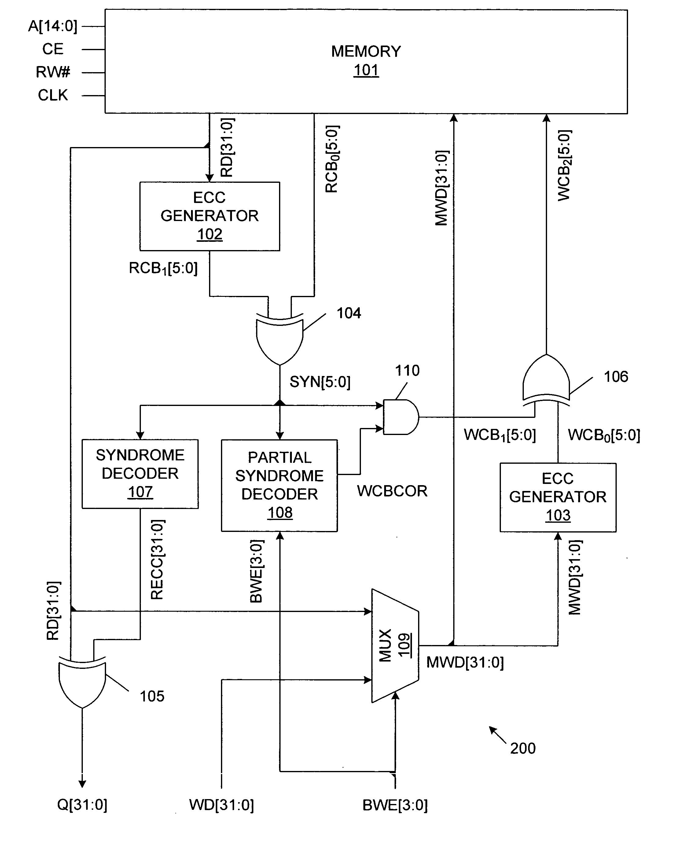
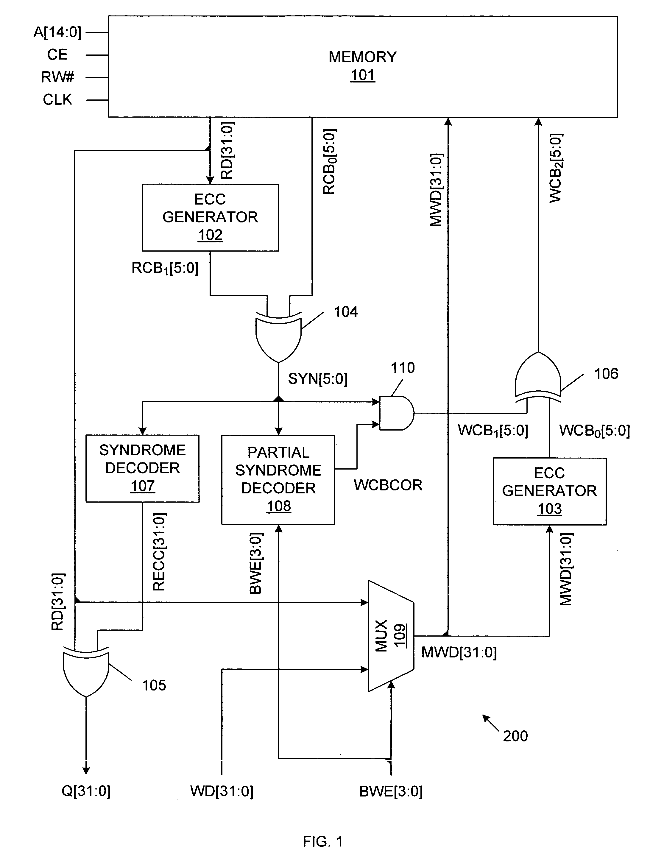
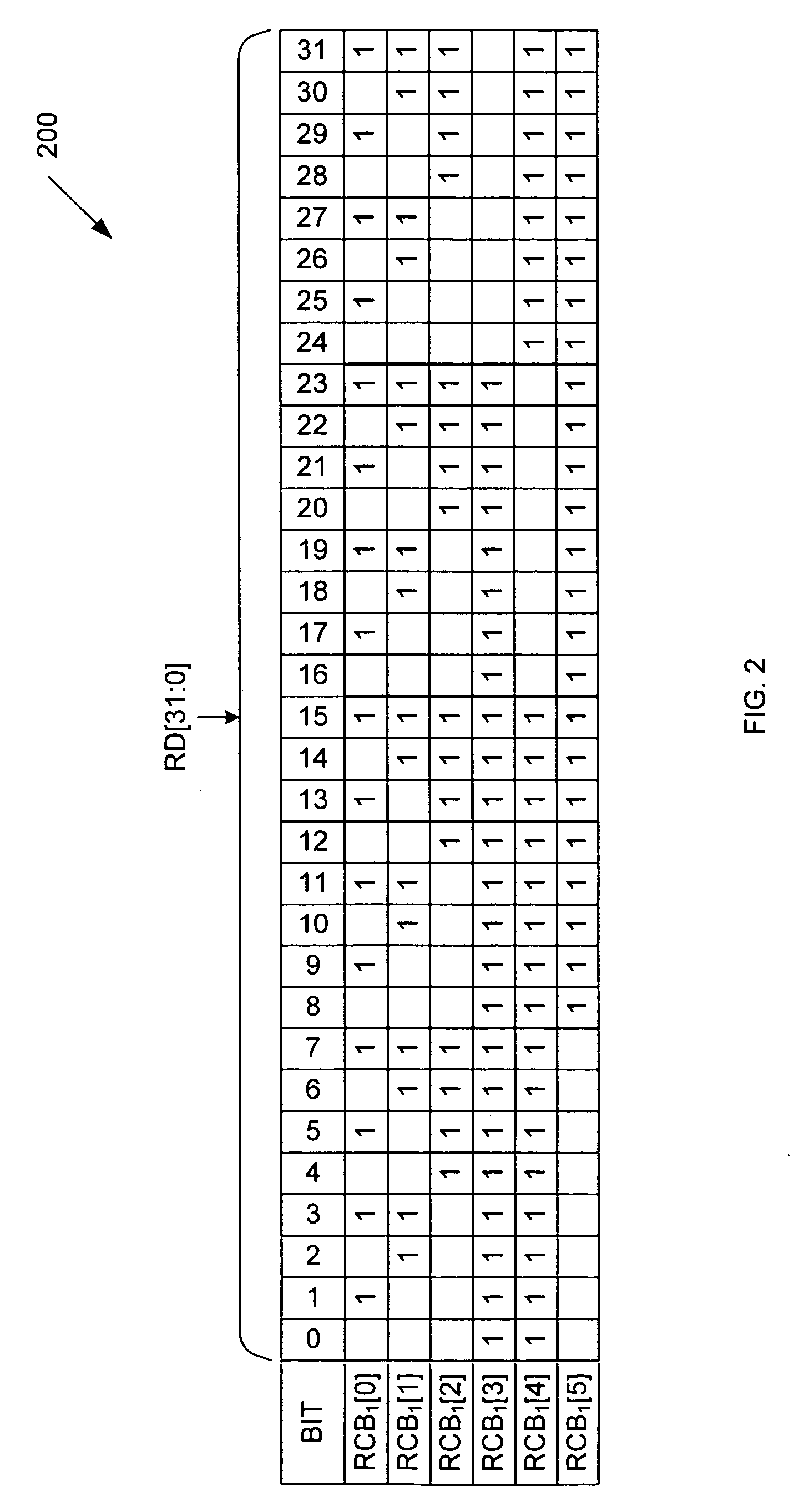
[0019]FIG. 1 is a block diagram of a memory system 100, which implements a partial-word write with predictive error correction in accordance with one embodiment of the present invention. Memory system 100 includes memory array 101, error correction code (ECC) generators 102-103, exclusive OR circuits 104-106, syndrome decoder 107, partial syndrome decoder 108, multiplexer circuit 109 and logical AND circuit 110. In the described embodiment, memory array 101 is organized as 32 k words of 32-bits each, and uses 6 check bits to facilitate single-bit error correction. However, other word sizes and check bit widths can be used in other embodiments.

[0020] As described in more detail below, memory system 100 supports byte-write transactions using a read-modify-write operation. Memory system 100 provides a standard interface similar to interfaces used in common synchronous SRAM systems. Thus, memory array 101 operates in response to an address signal A[14:0], a chip enable signal CE, a rea...


PUM


Abstract

Write check bits are generated in a predictive manner for partial-word write transactions in a memory system implementing error code correction. A read data word and associated read check bits are read from an address of the memory. If an error exists in a byte of the read data word, this byte is identified. At the same time, one or more bytes of the uncorrected read data word are merged with one or more bytes of a write data word, thereby creating a merged data word. Write check bits are generated in response to the merged data word. If the merged data word includes a byte of the read data word, which contains an error, the write check bits are modified to reflect this error. The merged data word and the modified (or unmodified) write check bits are then written to the address of the memory.

Description

RELATED APPLICATIONS [0001] The present application is related to pending U.S. patent application Ser. No. 10 / 645,861, “Transparent Error Correcting Memory” by Wingyu Leung, Kit-Sang Tam, Mikolaj Tworek and Fu-Chieh Hsu, which is a continuation in part of pending U.S. patent application Ser. No. 10 / 003,602, “Error Correcting Memory And Method of Operating Same” by Wingyu Leung and Fu-Chieh Hsu. The present invention is also related to U.S. Pat. No. 6,147,535, entitled “Clock Phase Generator for controlling operation of a DRAM Array” by Wingyu Leung.FIELD OF THE INVENTION [0002] The present invention relates to semiconductor memory systems, such as static random access memory (SRAM) systems or dynamic random access memory. (DRAM) systems. In particular, the present invention relates to a method and apparatus of error detection and correction in a semiconductor memory that supports partial-word write operations. RELATED ART [0003] Semiconductors memories such as DRAM and SRAM devices ...

Claims


Application Information

Patent Timeline
Patent Type & Authority Applications(United States)
IPC IPC(8): G11C29/00
CPCG06F11/1056G11C7/1006G11C11/4078
Inventor LEUNG, WINGYUTAM, KIT SANG
Owner INVENSAS CORP
Why Eureka
Try Eureka