Transistors having buried N-type and P-type regions beneath the source region and methods of fabricating the same

a technology of transistors and source regions, applied in the field of transistors, can solve the problems of limited power handling capability of such devices at higher operating frequencies, large heat generation of high power and high frequency transistors, and limited power handling capability of previously known jfets

Active Publication Date: 2006-06-15
CREE INC
View PDF34 Cites 13 Cited by
  • Summary
  • Abstract
  • Description
  • Claims
  • Application Information

AI Technical Summary

Benefits of technology

[0016] Some embodiments of the present invention provide a unit cell of a metal-semiconductor field-effect transistor (MESFET). The unit cell of the MESFET includes a MESFET including a source region, a drain region and a gate contact. The gate contact is between the source region and the drain region and on an n-type conductivity channel layer. A p-type conductivity region is provided beneath the source

Problems solved by technology

Previously, bipolar transistors and power metal-oxide semiconductor field effect transistors (MOSFETs) have been used for high power applications but the power handling capability of such devices may be limited at higher operating frequencies.
Junction field-effect transistors (JFETs) were commonly used for high frequency applications but the power handling capability of previously known JFETs may also be limited.
In turn, high power and high frequency transistors usually generate larger amounts of heat than small signal transistors.
Although these devices provide increased operating frequencies and moderately increased power handling capability, the relatively low breakdown voltage and the lower thermal conductivity of these materials

Method used


Image

  • Transistors having buried N-type and P-type regions beneath the source region and methods of fabricating the same
  • Transistors having buried N-type and P-type regions beneath the source region and methods of fabricating the same
  • Transistors having buried N-type and P-type regions beneath the source region and methods of fabricating the same

Examples


Embodiment Construction

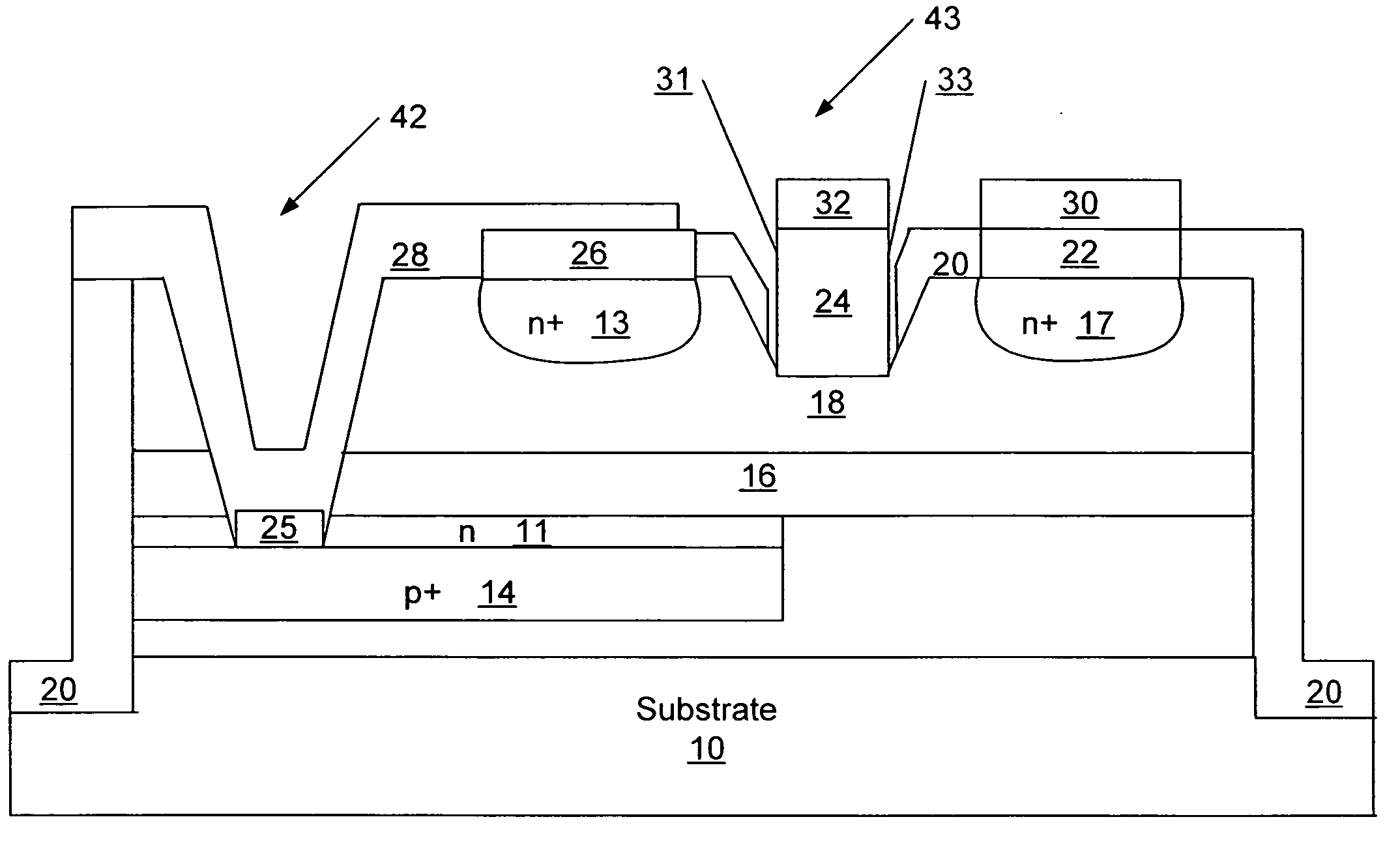
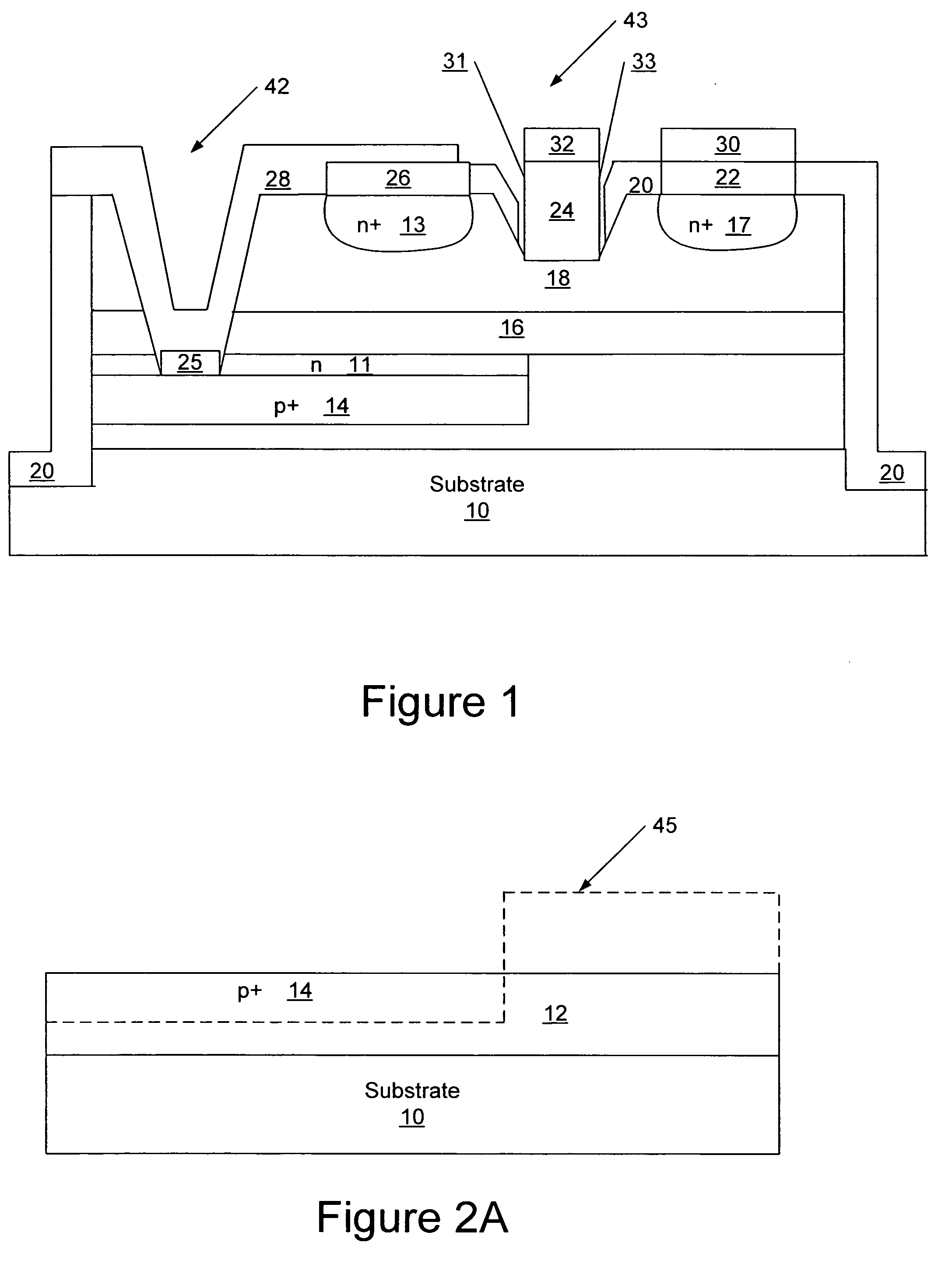
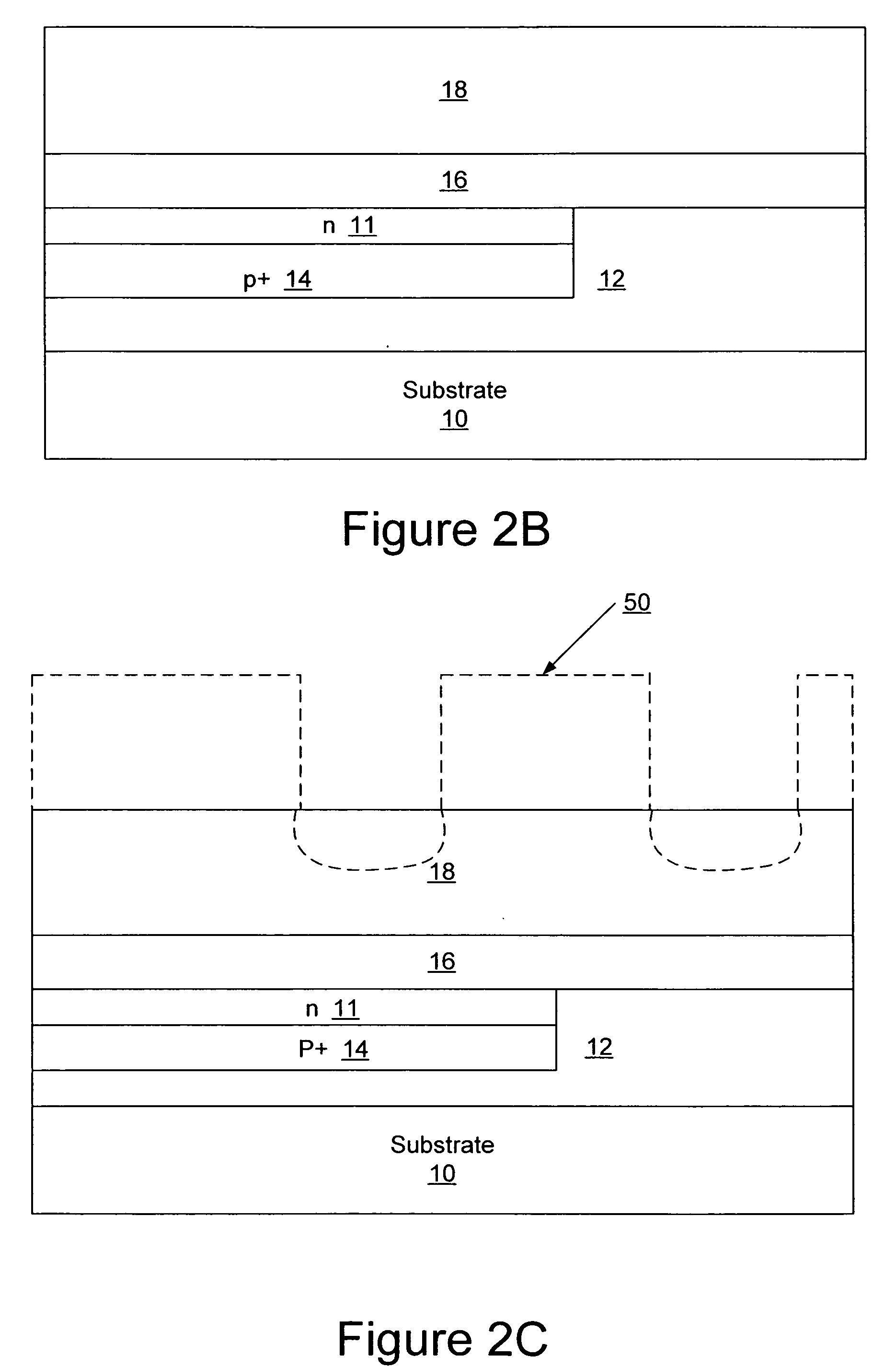
[0032] The invention is described more fully hereinafter with reference to the accompanying drawings, in which embodiments of the invention are shown. This invention may, however, be embodied in many different forms and should not be construed as limited to the embodiments set forth herein. Rather, these embodiments are provided so that this disclosure will be thorough and complete, and will fully convey the scope of the invention to those skilled in the art. In the drawings, the size and relative sizes of layers and regions may be exaggerated for clarity. It will be understood that when an element or layer is referred to as being “on”, “connected to” or “coupled to” another element or layer, it can be directly on, connected or coupled to the other element or layer or intervening elements or layers may be present. In contrast, when an element is referred to as being “directly on,”“directly connected to” or “directly coupled to” another element or layer, there are no intervening elem...


PUM


Abstract

The present invention provides a unit cell of a metal-semiconductor field-effect transistor (MESFET). The unit cell of the MESFET includes a source, a drain and a gate. The gate is disposed between the source and the drain and on an n-type conductivity channel layer. A p-type conductivity region is provided beneath the source and has an end that extends towards the drain. The p-type conductivity region is spaced apart from the n-type conductivity channel region and is electrically coupled to the source. An n-type conductivity region is provided on the p-type conductivity region beneath the source region and extending toward the drain region without extending beyond the end of the p-type conductivity region. Related methods of fabricating MESFETS are also provided.

Description

STATEMENT OF GOVERNMENT INTEREST [0001] This invention was made with Government support. The Government has certain rights in this invention.FIELD OF THE INVENTION [0002] The present invention relates to microelectronic devices and more particularly to transistors, for example, metal-semiconductor field-effect transistors (MESFETs). BACKGROUND OF THE INVENTION [0003] Electrical circuits requiring high power handling capability while operating at high frequencies such as radio frequencies, S-band and X-band have in recent years become more prevalent. Because of the increase in high power, high frequency circuits there has been a corresponding increase in demand for transistors that are capable of reliably operating at radio frequencies and above while still being capable of handling higher power loads. Previously, bipolar transistors and power metal-oxide semiconductor field effect transistors (MOSFETs) have been used for high power applications but the power handling capability of s...

Claims


Application Information

Patent Timeline
IPC IPC(8): H01L29/76
CPCH01L29/0619H01L29/1608H01L29/2003H01L29/41766H01L29/8128H01L21/18
Inventor SRIRAM, SAPTHARISHI
Owner CREE INC
Why Eureka
Try Eureka