In applications powered by single-
cell NiMH and alkaline batteries must operate with as little as 0.9V of
battery voltage, however, these limitations are more severe.
With such
low voltage conditions, power MOSFETs exhibit inefficient and unreliable operation, lacking the gate drive necessary to switch between their low-leakage “off” state and a low-resistance “on” state.
With manufacturing variations in their
threshold voltage, the
voltage the device turns-on, their resistance, current capability, and leakage characteristics render them virtually useless at such low-voltages.
While the
silicon power MOSFET has been successful in implementing switching
converters up to 2 MHz, their operation above that frequency is too inefficient to be commercially practical.
Unfortunately, a much higher
switching frequency is needed to eliminate the need for an
inductor, now the physically largest component in a power supply.
At 0.9V gate bias, that means the
transistor has only 0.4V
voltage overdrive above its threshold, inadequate to fully enhance the transistor's conduction.
Even in
lithium ion battery powered applications, power MOSFETs suffer from a number of limitations, especially those adversely impacting their efficiency in
high frequency switching applications above 2 MHz.
At low voltages, i.e. under 30V, a power MOSFETs
high input capacitance becomes a significant and even dominant component of
power loss in a switching converter.
Increasing the transistor's gate bias to reduce
on resistance adversely impacts gate drive switching losses.
Conversely reducing gate drive improves drive losses but increases resistance and conduction losses.
Even attempts to optimize or improve a power
MOSFET's design,
layout, and fabrication involve compromises.
The tradeoff between on-resistance
and gate drive losses limits the
maximum efficiency of a converter, becoming increasingly severe at lower operating voltages.
For example, the aforementioned tradeoff prevents Lilon-powered switching
converters from operating at frequencies over a few megahertz, not because they can't operate, but because their efficiency becomes too low.
Its ability to operate at low gate-drive voltages makes the MESFET potentially attractive as a power device, but also introduces certain yet unresolved challenges.
Of these challenges, the most significant problem is commercially available MESFETs are limited to the normally-on, or depletion-mode type.
Normally-on type switches are unfortunately not useful for
power switching applications.
As an alternative to wide bandgap materials,
silicon may be used, but
silicon's Schottky leakage characteristic is generally not attractive for power applications, especially when operation over temperature and self-heating are considered.
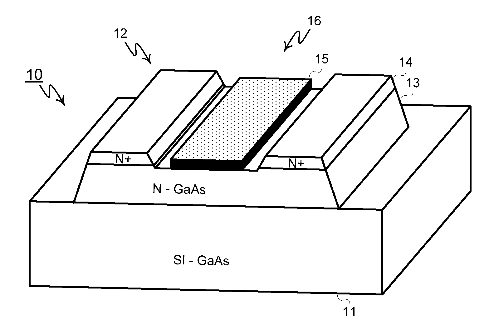
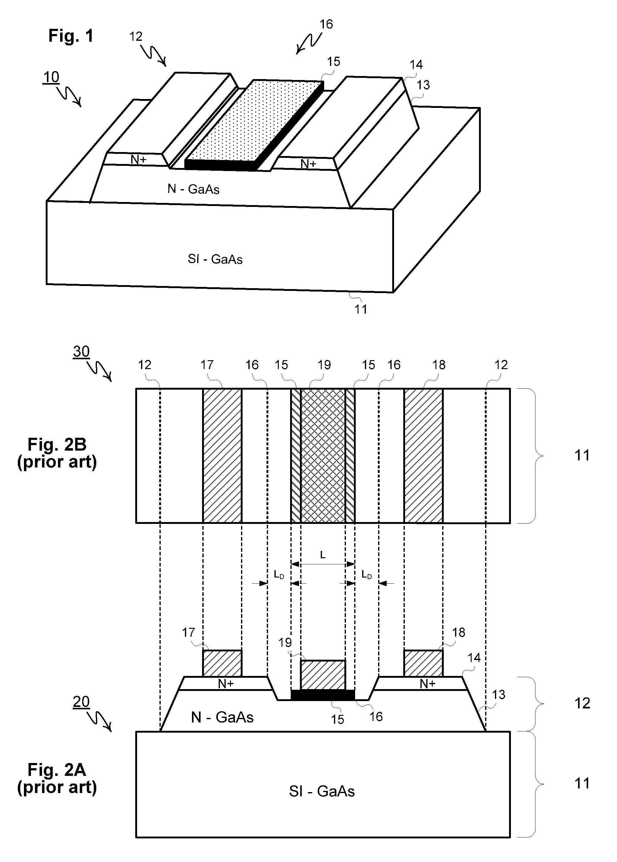
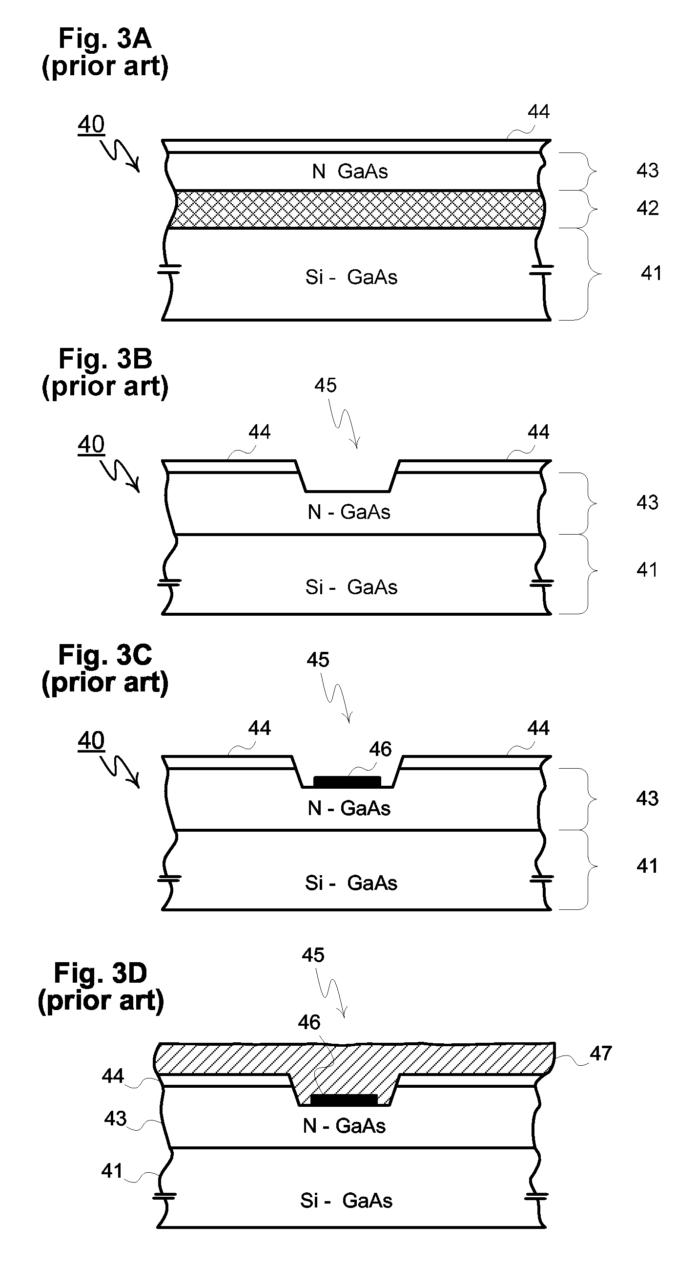
The mesa etch is required to isolate the device from other devices since GaAs and other III-V or binary-element crystals do not readily form insulating dielectrics through
thermal oxidation.
Because the device utilizes only a single metallization layer for
interconnection, the geometric
layout of the device remains limited compared to devices used in silicon integrated circuits.
In the event trench 54 is etched slightly deeper such that the
reverse bias of gate 55 fully depletes the epitaxial layer under the
trench gate, the magnitude of IDmin is reduced but because IDSS is not “zero”, the device remains a depletion mode device, not suitable for use as a power switch.
As a result enhancement-mode MESFETs were never commercialized.
Such devices, while not generally useful for power switch applications, are commonly used for RF switches in
cell phones.
While such device may still be used in small-
signal circuit applications (such as an
amplifier or
gain element), they are not useful as a power switch since they cannot be shut off, even with a high negative gate bias.
The combination of high electric fields and
high current densities in the vicinity of point 82 leads to localized carrier generation, avalanche, and hot carriers that can destroy the device.
The MESFET in its prior art form is therefore not suitable for
power switching applications because of its inability to survive even temporary over-voltage conditions.
Aside from certain fundamental frailties intrinsic to the device's present construction, commercially available MESFETs have other design limitations that further degrade their avalanche ruggedness.
Due to surface state charges, the origin of leakage current and the onset of avalanche will be most severe at the device surfaces, especially at the mesa edge at points A and B.
Even if a suitable power device is available to meet requisite ruggedness,
capacitance, and speed requirements of
high frequency DC-to-DC converters, other challenges exist, especially those relating to device-circuit interactions and tradeoffs.
In the prior art, for example, other challenges to implementing
high frequency DC-to-DC converters involve fast
shoot-through protection, sensing switch current, and minimizing
stray inductance of the converter components.
Crow-barring the battery input, i.e. shorting the battery terminals even for a moment, drains the battery of precious
stored energy, and in some instances may result in potentially dangerous spikes in current, overheating, or even a
fire hazard.
While the BBM interval (where both transistors are off) must be sufficiently long in duration to guarantee the
shoot through condition never occurs, extremely long duration BBM intervals lead to increased power losses since the current flowing through
inductor 103 must be carried by
diode conduction in either Schottky 105 or by the P-N
diode 107 intrinsic to
MOSFET 106.
Unfortunately at increasing frequencies, break before make circuit 109 becomes increasingly problematic for circuit implementations where the threshold voltages of the P-channel and N-channel transistors in the BBM buffer circuitry are not correlated to (i.e. do not “track”) the threshold of N-channel and P-
channel power transistors 101 and 106.
Even ignoring switching losses and poor efficiency, the variability of the BBM interval therefore sets a limitation in the maximum frequency of a converter.
If the power MOSFETs comprise discrete lateral
low voltage devices not correlated to the BBM buffer, accounting for
process variability practically limits BBM and converter operation to 2 MHz.
Moreover, lateral integrated silicon power MOSFETs suffer from an intrinsically poor tradeoff between on-resistance
and gate charge.
This tradeoff limits their use to converter switching rates of a few megahertz, frequencies too low to eliminate the need for large inductors in switch-mode power supplies.
In such cases, acceptable operation even at 1 MHz can be challenging since discrete devices do not necessarily share the same
wafer during production, exhibit statistically uncorrelated threshold voltages, and have high gate-charge for a given on-resistance.
Similarly adapting other
semiconductor devices such as discrete MESFETs face similar challenges since MESFET characteristics do not track accurately from lot to lot.
In summary, whenever BBM circuitry cannot be constructed using the same process as the power stage, prior art switching converter methods do not predictably operate at high frequencies and short BBM intervals.
The problem is further exacerbated since vertical power devices themselves have uncorrelated threshold voltages, i.e. are not co-fabricated on the same
wafer.
The substitution of discrete power
MOSFET with power MESFETs faces the same issues, namely that the devices cannot be monolithically integrated without isolation and that their threshold voltages will therefore not track one another.
Current sensing in DC-to-DC converters further complicates high frequency operation.
Unfortunately, even ignoring the expense of such an approach, the 40% larger MOSFET also exhibits a 40% increase in its
gate capacitance and gate charge, i.e. 1.4 times the QG of the
original device.
Unfortunately, this and similar current sense methods are only useful if the main and sense MOSFETs are manufactured in a process capable of integrating multiple isolated device—a feature not always available in power transistor fabrication.
Furthermore, since many III-V and II-VI
compound semiconductor materials such as
gallium-
arsenide cannot be oxidized or do not form high quality dielectrics; device-isolation requires expensive mesa etch processes.
Large step heights resulting from the mesa etch also make the process of on-
chip metal interconnection difficult or impossible due to the resulting non-planar surface.
The less these components are integrated, the greater the dimensions and the larger the magnitude of stray inductances will be.
Not all inductances have equally adverse effects on converter operation.
If source
inductance (not shown) is also present, the varying source potential can make it difficult to rapidly turn off a conducting device, and thereby contribute to unwanted
power loss, lower efficiency, and an overall increase in converter power dissipation.
But vertical power MOSFET cannot be monolithically integrated in this manner, nor can
present day MESFETs.

