On-chip ESD protection circuit using enhancement-mode HEMT/MESFET technology

a protection circuit and enhancement-mode technology, applied in the direction of transistors, electrical devices, arrangements responsive to excess voltage, etc., can solve the problems of parasitic impedance and capacitance of traditional protection devices that can distort and deteriorate signal integrity, reduce signal magnitude and magnitude of power amplifiers, and save chip space and product costs. , the effect of reducing power consumption

Active Publication Date: 2008-04-03
WIN SEMICON
View PDF5 Cites 31 Cited by
  • Summary
  • Abstract
  • Description
  • Claims
  • Application Information

AI Technical Summary

Benefits of technology

[0008]In the present invention, an ESD protection circuit comprising a trigging diode string and a shunting transistor is disclosed. The triggering diode string can trigger the shunting transistor to conduct ESD current away rapidly when it is suffered a voltage spike. In the present invention, because the protected RF circuit is in HEMTs / MESFETs, the shunting transistor is therefore replaced by a HEMT / MESFET for on-chip ESD protection circuit design. An on-chip ESD protection circuit can save the chip space and product cost, and lower down power consumption. Because the on-chip ESD protection circuit in HEMTs / MESFETs chip must be at nonconducting configuration under normal operating voltage, a triggering diode string and a normally off enhancement mode (E-mode) HEMT / MESFET having its gate coupled to the triggering diode string are necessary. Additionally, the dual-gate design in the present invention reduces the parasitic capacitance of ESD protection for RF circuit performance without expanding device size.

Problems solved by technology

Therefore, an integrated circuit (IC) connected to external ports is vulnerable to ESD damaging pulses from the operating environment and peripherals.
However, at the much higher data rates of USB 2.0, IEEE 1394, and digital visual interface (DVI) and at radio frequency (RF) operation, the parasitic impedance and capacitance of traditional protection devices can distort and deteriorate signal integrity.
The parasitic effect may decrease signal magnitude and magnitude of power amplifier, narrow the applied bandwidth, and decrease the signal to noise ratio.
Because their epitaxy growth is totally different with HBT's, the on-chip ESD protection circuit with HBT Darlington pair is not suitable for RF circuit in pHEMTs or MESFETs anymore.

Method used


Image

  • On-chip ESD protection circuit using enhancement-mode HEMT/MESFET technology
  • On-chip ESD protection circuit using enhancement-mode HEMT/MESFET technology
  • On-chip ESD protection circuit using enhancement-mode HEMT/MESFET technology

Examples


Embodiment Construction

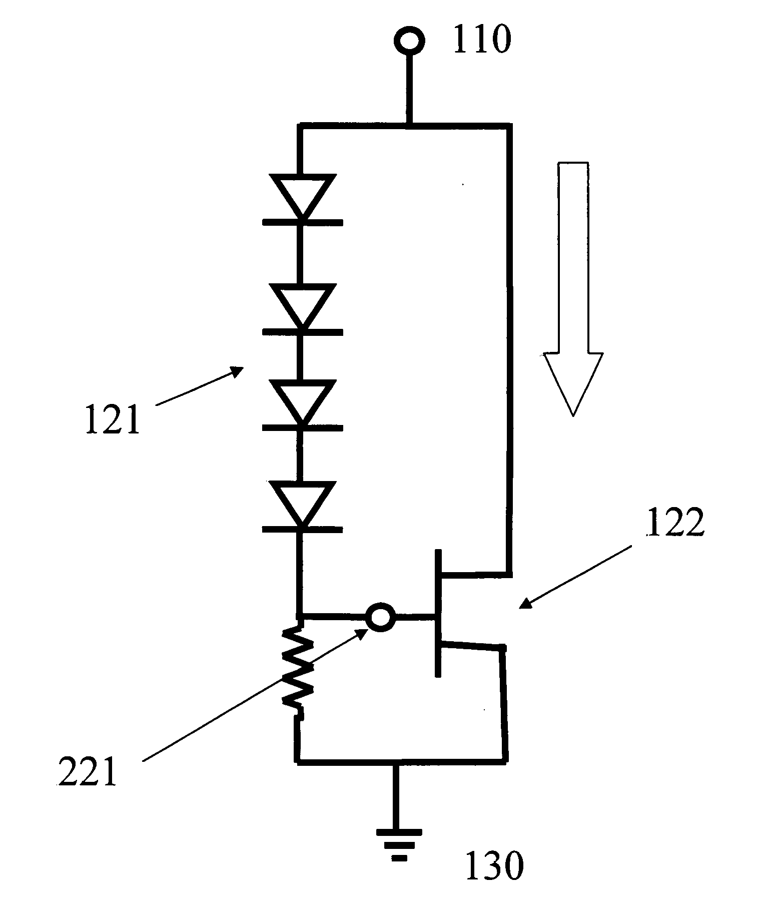
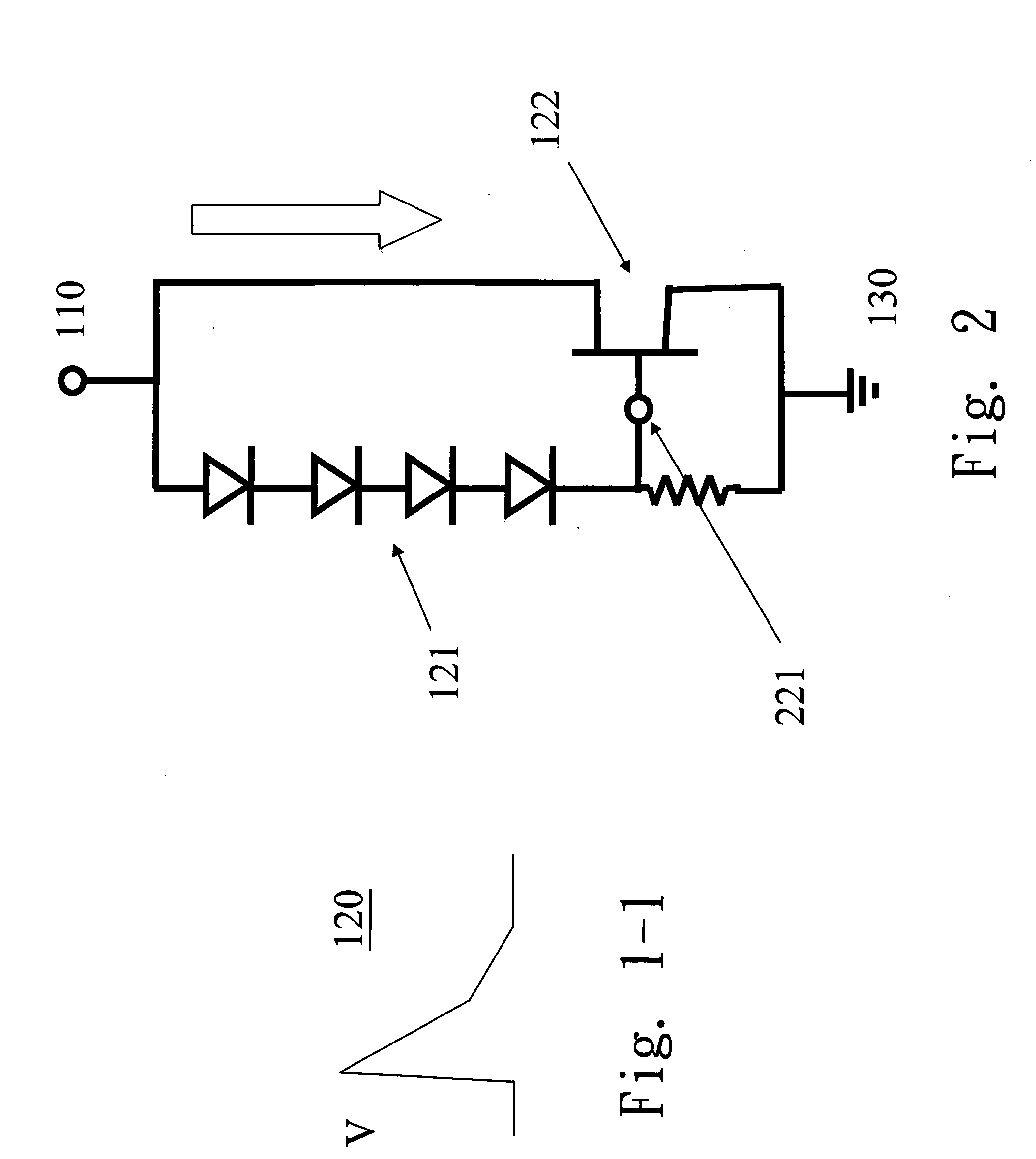
[0018]A shunting ESD protection circuit of the present invention is simply shown on FIG. 1. The ESD protection circuit connected between a pad point 110 to the main RF circuit input and a ground point 130 to ground comprises a triggering diode string121 and a ESD shunting apparatus 122. The working principle of the shunting ESD protection circuit is to rapidly conduct the ESD current to ground point when the unexpected voltage spike between the pad point and the ground point is happened (as FIG. 1-1), and to be a nonconducting circuit when the voltage between the pad point and the ground point is in normal operation. FIG. 2 shows the detail working sequence. When a voltage spike between the pad point and the ground point is larger than the forward bias threshold of the triggering diode string, the voltage between gate 221 of the ESD shunting apparatus and the ground point becomes positive and switches the ESD shunting transistor to be conducted. The conducted ESD shunting apparatus ...


PUM


Abstract

An on-chip circuit for protection against electrostatic discharge (ESD) is disclosed. Unlike conventional ESD protection circuit using high turn-on voltage diode string, the circuit uses a plural of enhancement-mode HEMT / MESFET triggered by a shorter diode string to shunt large ESD current for protected susceptive RF circuit. Further, by using dual-gate technology of enhancement-mode HEMT / MESFET, the on-chip ESD protection circuit has the less parasitic capacitance without expanding device size for vulnerable RF circuit.

Description

BACKGROUND OF THE INVENTION[0001]1. Field of the Invention[0002]The present invention relates to an electrostatic discharge (ESD) protection circuit on semiconductor chip, and more particular on III / V compound semiconductor chip, wherein a shunt circuit using enhancement-mode HEMT / MESFET technology for protection against ESD is connected between integrated circuit (IC) pad and ground.[0003]2. Description of the Prior Art[0004]An electrostatic discharge (ESD) event is the energy transfer between two bodies at different electrostatic potentials, either through contact or via an ionized ambient discharge (a spark). Therefore, an integrated circuit (IC) connected to external ports is vulnerable to ESD damaging pulses from the operating environment and peripherals. For the fact of ESD event, four models of ESD, Human-Body Model (HBM), Machine Model (MM), Charge-Device Model (CDM), and Field-Induced Model (FIM), are built to present the real damage to IC from ESD event. In order to protec...

Claims


Application Information

Patent Timeline
Patent Type & Authority Applications(United States)
IPC IPC(8): H02H9/00
CPCH01L27/0285
Inventor LIN, CHENG-KUOWANG, YU-CHILIU, JOSEPHSUN, JEAN
Owner WIN SEMICON
Why Eureka
Try Eureka