Vertical field effect transistor and method for fabricating the same

a technology of vertical field and transistor, which is applied in the direction of semiconductor devices, electrical devices, nanotechnology, etc., can solve the problems of increasing the price of exposure systems and photomasks, the difficulty of selectively forming nanotubes with the desired degree of conductivity, and the limit of the size reduction realized by modifying photolithographic process parameters. to achieve the effect of increasing the number of devices integrated together

Inactive Publication Date: 2006-06-15
JOLED INC
View PDF11 Cites 90 Cited by
  • Summary
  • Abstract
  • Description
  • Claims
  • Application Information

AI Technical Summary

Benefits of technology

[0016] In order to overcome the problems described above, preferred embodiments of the present invention provide a vertical field effect transistor, which contributes to significantly increasing the number of devices integrated together per unit area, and also provide a method for fabricating such a field effect transistor.

Problems solved by technology

However, such a size reduction realized by modifying photolithographic process parameters is going to reach a limit.
In addition, the smaller the minimum patterning size, the higher the prices of exposure systems and photomasks tend to be.
Thus, it is difficult to selectively form nanotubes with a desired degree of conductivity.
According to the conventional techniques disclosed in the documents mentioned above, however, it is difficult to control the direction and positions of nanowires growing.
Nevertheless, that method provides a narrow control range, requires a complicated manufacturing process and therefore, cannot be used effectively to make LSIs or TFTs.
Accordingly, this technique cannot be applied effectively to mass-producing large-scale circuits or circuits including multiple types of elements.
According to the positional control by the photolithographic technique on the other hand, it is difficult to reduce the dimensions below the exposure limit.
For that reason, this technique is not suitable to forming a nanometer scale device.
Also, it is very difficult to grow nanowires like a blanket and then selectively remove unnecessary ones of the nanowires.
Thus, the dimensions of a transistor cannot be reduced below the limit of the photolithographic process.

Method used


Image

  • Vertical field effect transistor and method for fabricating the same
  • Vertical field effect transistor and method for fabricating the same
  • Vertical field effect transistor and method for fabricating the same

Examples


embodiment 1

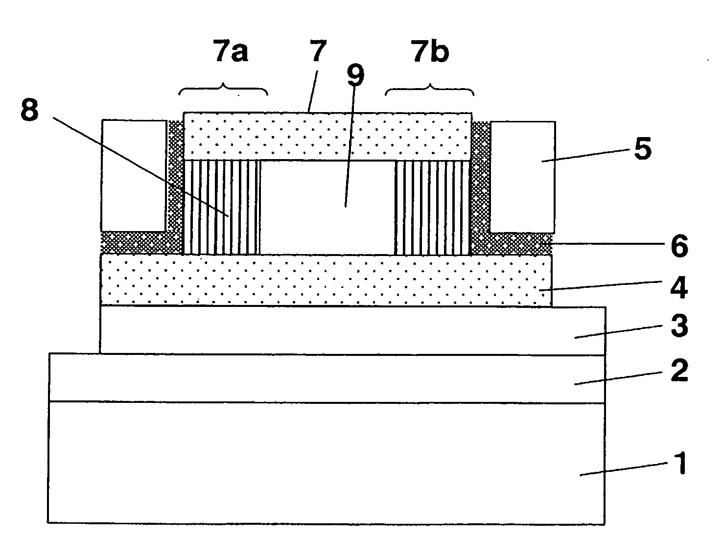
[0077] A vertical field effect transistor according to a first specific preferred embodiment of the present invention will be described with reference to FIGS. 6A and 6B. FIG. 6A is a top view schematically illustrating the arrangement of the vertical field effect transistor of this preferred embodiment (in which the illustration of the upper electrode 7 is omitted) and FIG. 6B is a cross-sectional view thereof as viewed on the plane VIb-VIb shown in FIG. 6A.

[0078] The transistor of this preferred embodiment is a vertical thin-film transistor (which will be abbreviated herein as a “vertical TFT”) provided over a glass substrate 1. In the nanowires of its channel region 8, carriers (electrons or holes) move perpendicularly to the principal surface of the glass substrate 1.

[0079] In this preferred embodiment, the channel region 8 is made of a bundle of Ge nanowires doped with a p-type dopant, and vertically connects together a lower electrode 4 functioning as drain region and an upp...

embodiment 2

[0108] Hereinafter, a vertical field effect transistor according to a second specific preferred embodiment of the present invention will be described with reference to FIG. 10 and FIGS. 11A through 11D.

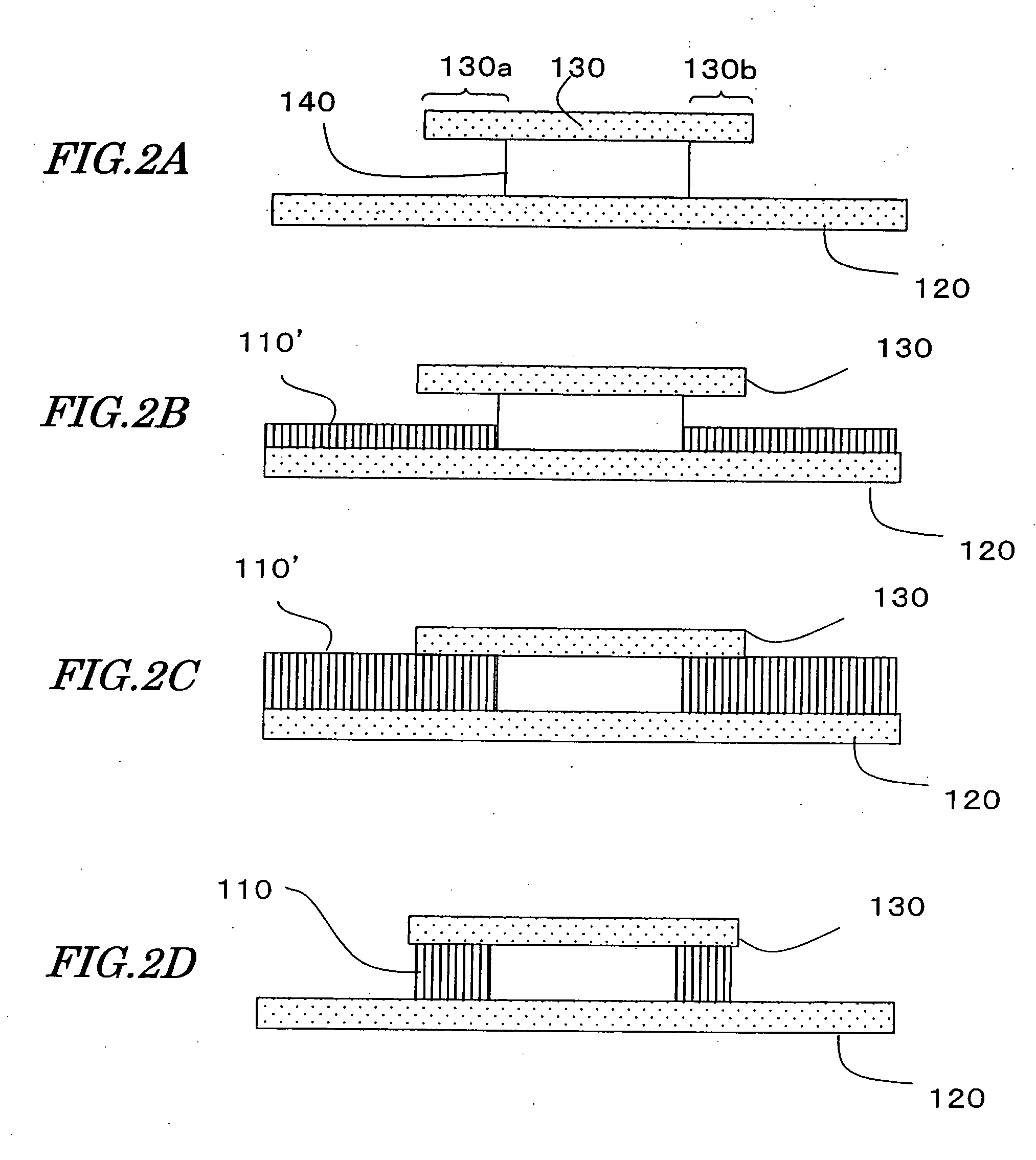
[0109] The vertical field effect transistor shown in FIG. 10 basically has the same configuration as the counterpart of the first preferred embodiment described above. Their difference lies in the shape and the patterning method of the lower electrode 4.

[0110] Hereinafter, a method for fabricating the vertical field effect transistor of this preferred embodiment will be described with reference to the accompanying drawings.

[0111] First, as shown in FIG. 11A, a silicon dioxide film 2, a transparent conductive film 3, a first conductor film 4′ to be the lower electrode 4, an insulating film 9′, and a second conductor film 7′ to be the upper electrode 7 are stacked in this order on an insulating substrate 1.

[0112] Next, as shown in FIG. 11B, the second conductor film 7′, insulating f...

embodiment 3

[0117] Hereinafter, a configuration for a vertical field effect transistor according to still another preferred embodiment of the present invention will be described with reference to FIGS. 12A and 12B.

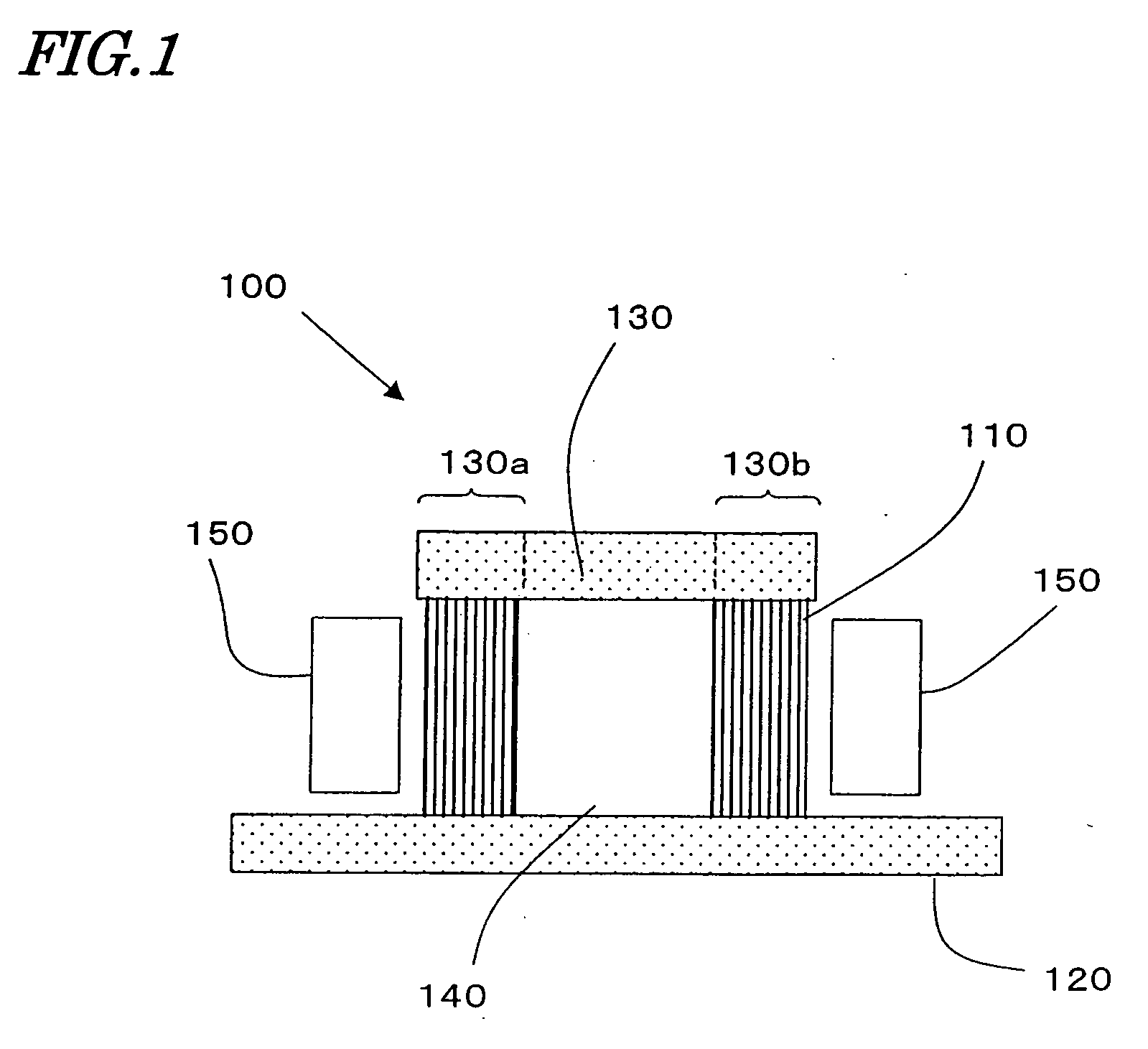
[0118] Unlike the vertical field effect transistor 100 shown in FIG. 1, the vertical field effect transistor 160 shown in FIG. 12A includes a cylindrical gate electrode 150 that extends vertically through the center of the dielectric portion 140. In the other respects, the transistors 160 and 100 have the same configuration.

[0119] As in the upper electrode 130 shown in FIG. 1, the upper electrode 130 shown in FIG. 12A is also located over the lower electrode 120 with the dielectric portion 140 interposed between them and also has an overhanging portion 130a, 130b that sticks out laterally from the upper surface of the dielectric portion 140. However, the upper electrode 130 shown in FIG. 12A has an opening, which is provided at the center to connect the gate electrode 150 to a line ...


PUM


Abstract

A vertical field effect transistor includes: an active region with a bundle of linear structures functioning as a channel region where electric carriers are transported; a lower electrode, connected to the bottom of the active region and functioning as one of source and drain regions; an upper electrode, connected to the top of the active region and functioning as the other of the source and drain regions; a gate electrode for controlling the electric conductivity of at least a portion of the bundle of linear structures included in the active region; and a gate insulating film arranged between the active region and the gate electrode to electrically isolate the gate electrode from the bundle of linear structures. The transistor further includes a dielectric portion between the upper and lower electrodes. The upper electrode is located over the lower electrode with the dielectric portion interposed and includes an overhanging portion that sticks out laterally from over the dielectric portion. The active region is located right under the overhanging portion of the upper electrode.

Description

[0001] This is a continuation of International Application PCT / JP2005 / 017830, with an international filing date of Sep. 28, 2005. BACKGROUND OF THE INVENTION [0002] 1. Field of the Invention [0003] The present invention relates to a vertical field effect transistor having an active region, which is made of a bundle of linear structures such as nanowires or carbon nanotubes that function as a channel region. The present invention also relates to a method for fabricating a vertical field effect transistor, which can provide nanowires on a region to be an active region such that the nanowires and the channel region are self-aligned with each other. [0004] 2. Description of the Related Art [0005] Transistors used in large-scale integrated circuits (LSIs) and thin-film transistors (TFTs) used in flat panel displays are all classified as field effect transistors (FETs) according to their operating principles. And the performance of those transistors has been enhanced by reducing their dim...

Claims


Application Information

Patent Timeline
Patent Type & Authority Applications(United States)
IPC IPC(8): H01L29/76
CPCB82Y10/00H01L29/0665H01L29/0673H01L29/0676H01L29/1606H01L29/42384H01L29/7781H01L29/78642H01L29/78696Y10S977/938
Inventor KAWASHIMA, TAKAHIROSAITOH, TOHRUTAKAGI, TAKESHI
Owner JOLED INC
Why Eureka
Try Eureka