Semiconductor package structure and method for fabricating the same

a technology of semiconductors and package structures, applied in the direction of semiconductor devices, semiconductor/solid-state device details, electrical apparatus, etc., can solve the problems of interface integration, increase the possibility of affecting the reliability of fabrication, increase the fabrication cost, etc., and achieve the effect of long fabrication time, low reliability, and increased fabrication cos

Inactive Publication Date: 2006-06-15
PHOENIX PRECISION TECH CORP
View PDF3 Cites 18 Cited by
  • Summary
  • Abstract
  • Description
  • Claims
  • Application Information

AI Technical Summary

Benefits of technology

[0015] The circuit board can be a double-layer or multi-layer circuit board, and is subsequently mounted on the carrier incorporated with the semiconductor chip by means of the conductive adhesive layer and the dielectric layer. This can eliminate the prior-art drawbacks such as complex fabrication processes, increased fabrication cost, long fabrication time and low reliability for a conventional semiconductor package. Further, the above arrangement can also avoid a loss to the cost and material caused by an overall package being found defective due to any defective build-up layer being formed during performing subsequent build-up processes on the carrier mounted with the semiconductor chip. Moreover, the circuit board can be preformed and in advance tested, which can prevent a loss to the cost and material caused by a defective product being examined and detected only after integration with the chip is complete, such that the fabrication rate can be increased to facilitate mass production.
[0016] Therefore, by the semiconductor package structure and the method for fabricating the same proposed in the present invention, at least one semiconductor chip having a plurality of electrode pads on a surface thereof is received in a cavity of a carrier, such that an overall thickness of the semiconductor package can be reduced to satisfy the requirement of profile miniaturization. Then, a dielectric layer is disposed on the carrier and the semiconductor chip, and is formed with a plurality of vias therein. A circuit layer and a plurality of conductive structure are formed on a surface of the dielectric layer and in the vias, and are electrically connected to the electrode pads of the semiconductor chip. Subsequently, a conductive adhesive layer and a circuit board having a plurality of conductive pads formed on a surface thereof are mounted on the dielectric layer. The conductive pads of the circuit board are electrically connected to the circuit layer and the conductive structures of the dielectric layer by conductive adhesive posts of the conductive adhesive layer, and are further electrically connected to the electrode pads of the semiconductor chip, so as to form a semiconductor package structure integrated with the carrier, the semiconductor chip and the circuit board therein. This combines chip carrier manufacture and a semiconductor packaging technique, and provides more flexibility to satisfy clients' requirements, as well as simplifies the semiconductor fabrication processes and an interface integration problem. Further in the present invention, electrical performances of the product can be improved, the fabrication processes can be simplified, and a loss to the yield can be reduced, thereby overcoming the drawbacks in the prior art.

Problems solved by technology

This not only increases the fabrication cost but also may raise the possibility of affecting reliability in fabrication.
These fabrication processes of the semiconductor device involve different manufacturers (including the chip carrier manufacturer and the semiconductor packaging manufacturer), which are complicated in practice and have difficulty in interface integration.
Moreover, if the client wishes to alter the functional design of the semiconductor device, this would involve further complicated changes and interface integration, thereby not providing flexibility in alteration and not satisfying the economical concern.
However, if any of the build-up layers is defective, it cannot be detected until the final build-up structure being tested.
This thereby causes a serious loss and makes mass production time-ineffective and cost-ineffective to implement, such that the mass production would be adversely affected as a consequence.

Method used


Image

  • Semiconductor package structure and method for fabricating the same
  • Semiconductor package structure and method for fabricating the same
  • Semiconductor package structure and method for fabricating the same

Examples


Embodiment Construction

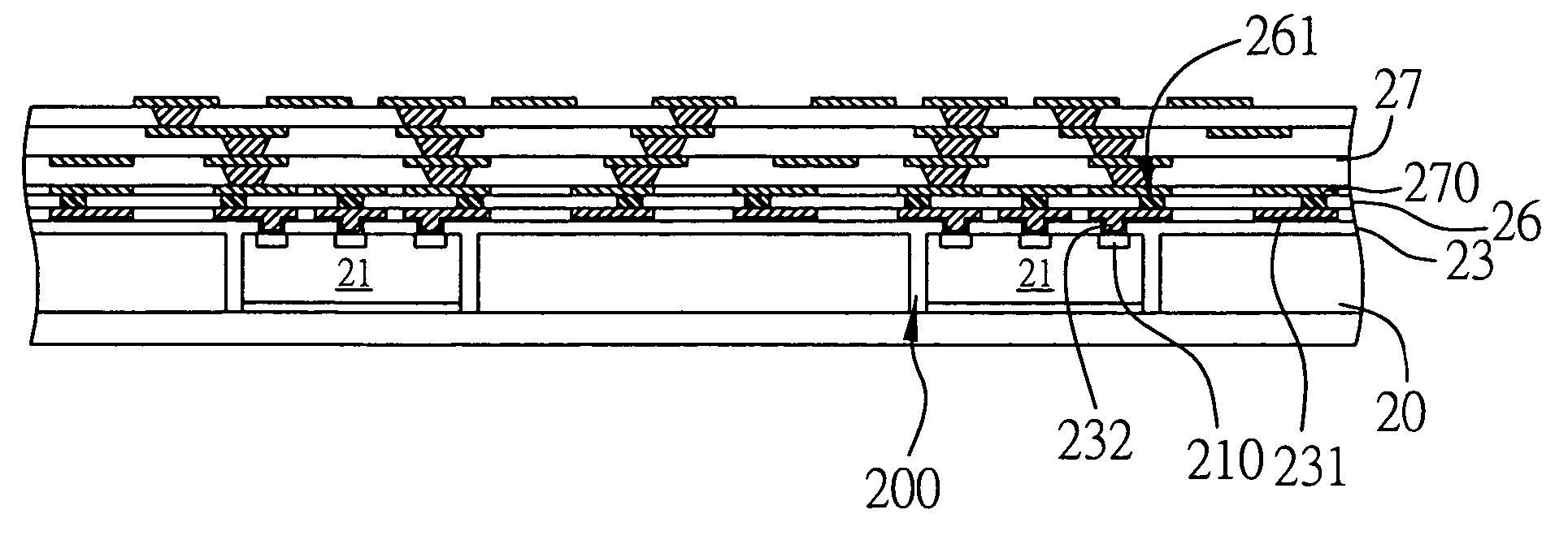
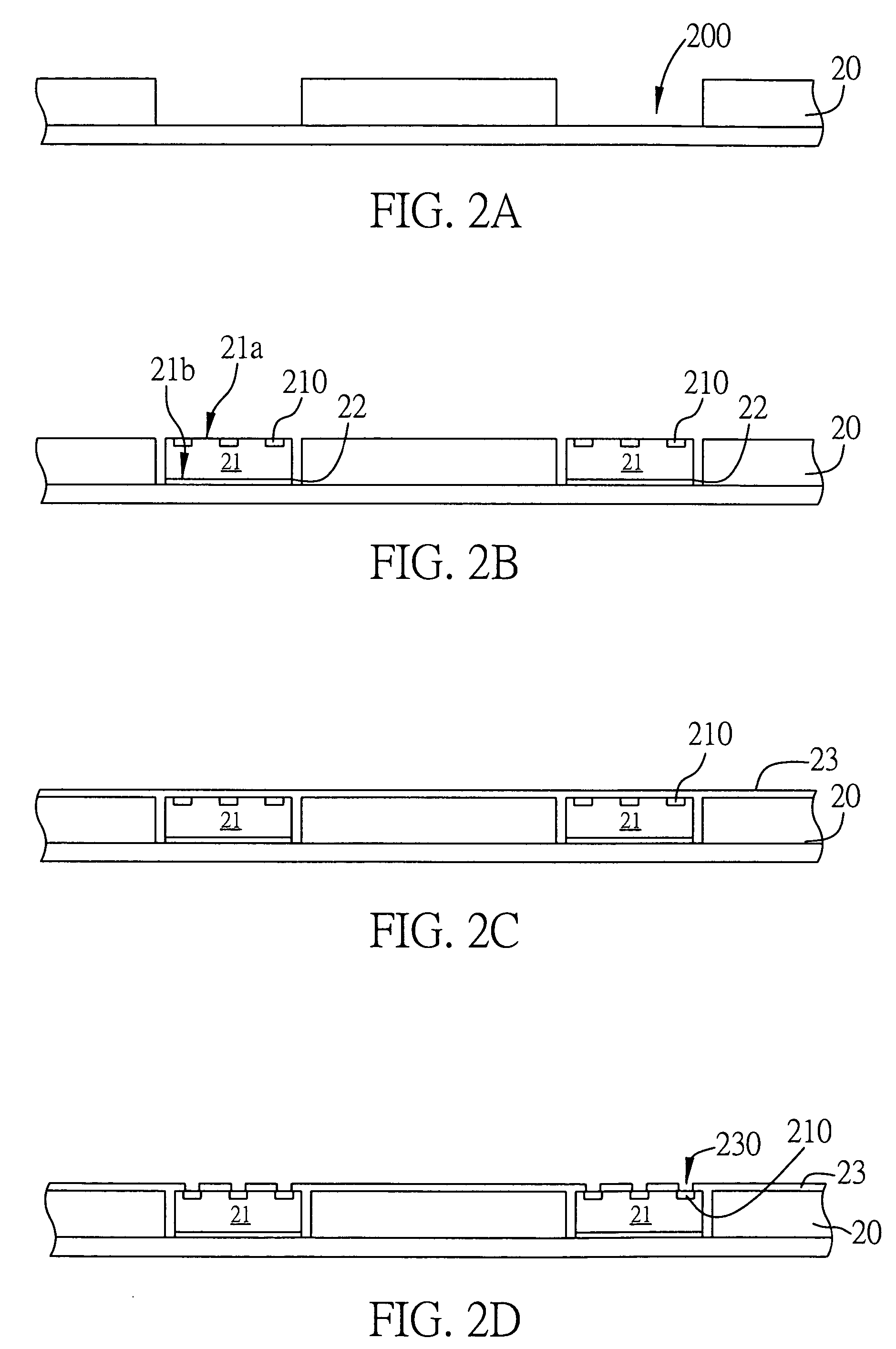
[0020]FIGS. 2A to 2J are cross-sectional schematic diagrams showing procedural steps of a method for fabricating a semiconductor package structure according to the present invention.

[0021] Referring to FIG. 2A, firstly, a carrier 20 having at least one cavity 200 is provided, such that at least one passive or active component such as semiconductor chip can be subsequently mounted in the cavity 200. The carrier 20 can be a metal plate, a ceramic plate or a circuit board. Alternatively, the carrier 20 having the cavity 200 can also be a combined structure of a heat sink and a circuit board with a cavity.

[0022] Referring to FIG. 2B, a non-active surface 21b of at least one semiconductor chip 21 is mounted in the cavity 200 of the carrier 20 via an adhesive layer. An active surface 21a of the semiconductor chip 21 is formed with a plurality of electrode pads 210 thereon.

[0023] Referring to FIG. 2C, a circuit build-up process is performed on the carrier 20 and the semiconductor chip 2...


PUM


Abstract

A semiconductor package structure and a method for fabricating the same are proposed. A carrier having at least one cavity is provided. At least one semiconductor chip having electrode pads is mounted in the cavity. A dielectric layer is applied on the carrier and the chip, and has vias for exposing the electrode pads of the chip. A circuit layer and conductive structures are formed on the dielectric layer and in the vias, wherein the conductive structures are electrically connected to the electrode pads of the chip. A conductive adhesive layer having conductive adhesive posts and a circuit board having conductive pads thereon are provided. The circuit board is mounted on the carrier via the conductive adhesive layer. The conductive pads of the circuit board are electrically connected to the circuit layer by the conductive adhesive posts and are further electrically connected to the electrode pads of the chip.

Description

FIELD OF THE INVENTION [0001] The present invention relates to semiconductor package structures and methods for fabricating the same, and more particularly, to a package structure capable of integrating a carrier, a semiconductor chip and a circuit board therein, and a method for fabricating the package structure. BACKGROUND OF THE INVENTION [0002] Along with the development of semiconductor packaging technology, different types of semiconductor devices have been produced. Ball Grid Array (BGA) is an advanced semiconductor packaging technique, which is characterized in the use of a substrate for mounting a semiconductor chip on a front side thereof, and implanting a grid array of solder balls on a back side thereof using a self-alignment technique. This allows more input / output (I / O) connections to be accommodated on the same unit area of a chip carrier e.g. the substrate so as to satisfy the requirement of high integration for the semiconductor chip, and the entire package unit can...

Claims


Application Information

Patent Timeline
Patent Type & Authority Applications(United States)
IPC IPC(8): H01L23/48H01L23/28H01L23/538
CPCH01L23/5389H01L24/19H01L24/24H01L2224/04105H01L2224/20H01L2224/24227H01L2924/01029H01L2924/14H01L2924/15153H01L2924/15165H01L2924/1517H01L2924/15311H01L2924/01033H01L2924/01047
Inventor HSU, SHIH-PING
Owner PHOENIX PRECISION TECH CORP
Why Eureka
Try Eureka