Method of fabricating mold for glass press
a mold and glass press technology, applied in the field of glass press mold fabrication, can solve the problems of not being able to form a minute structure, not being able to meet the needs of glass press mold material, and unable to process carbid
- Summary
- Abstract
- Description
- Claims
- Application Information
AI Technical Summary
Benefits of technology
Problems solved by technology
Method used
Image
Examples
example
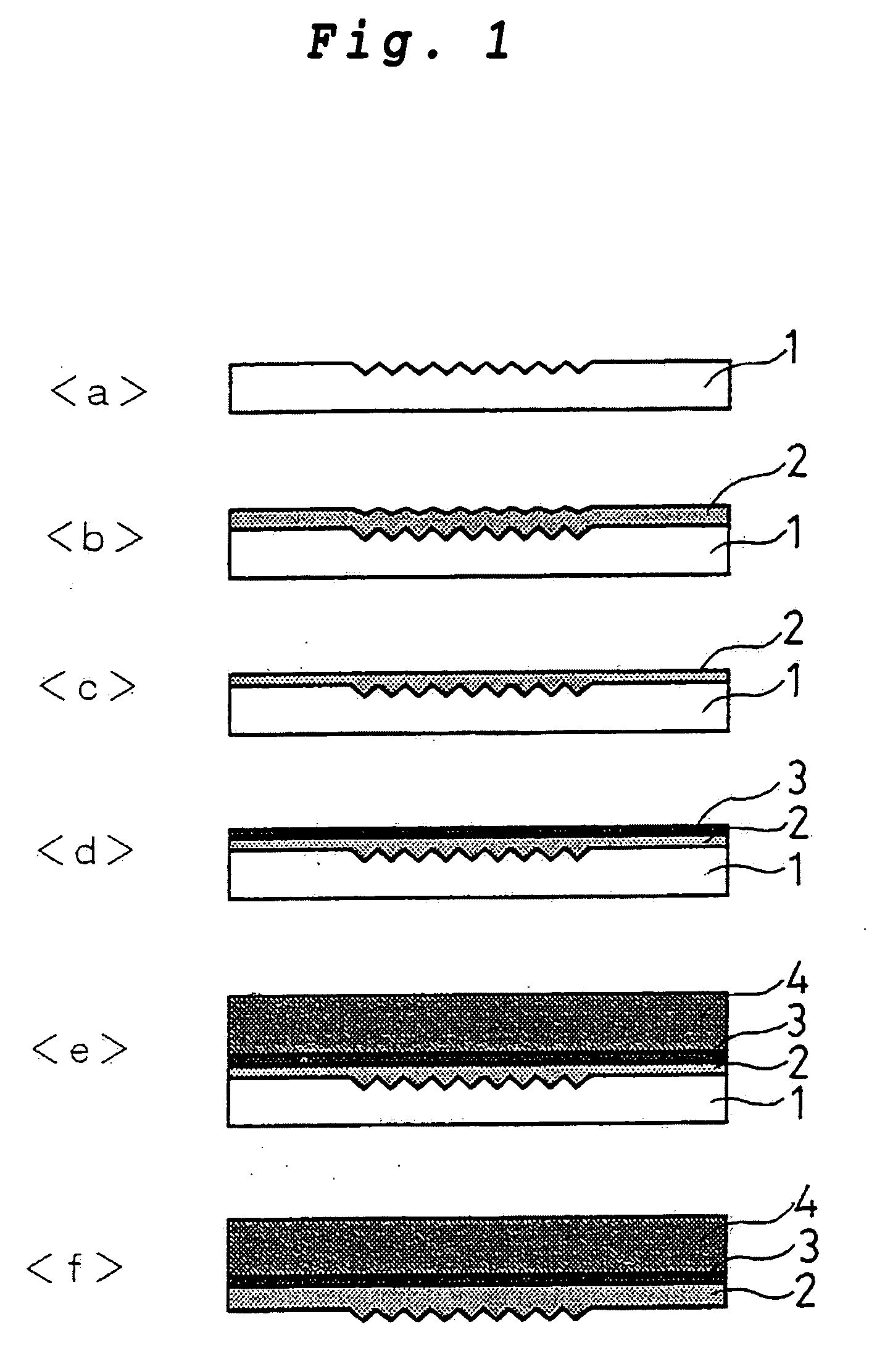
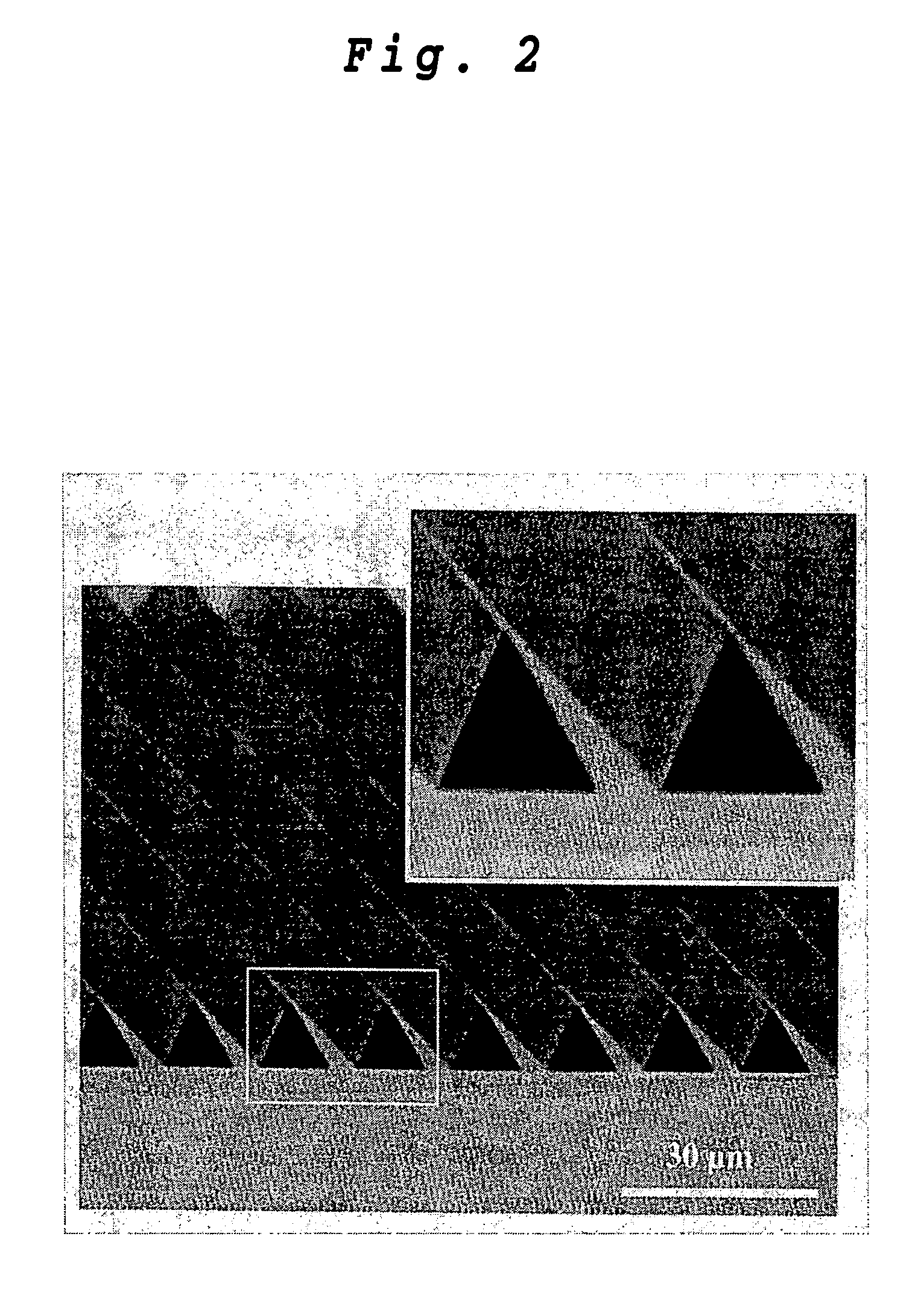
[0019] A silicon carbide was deposited by a 50 μm thickness on a silicon mold with a plurality of minute triangular grooves formed adjacently and parallel with each other on the surface by the atmospheric pressure CVD. Then, a 500 μm thickness silicon carbide substrate was bonded to the silicon carbide via a 0.5 μm thickness nickel thin film. The bonding conditions were 900° C. and 0.5 hour. Thereafter, the silicon mold was etched by a liquid mixture of a hydrofluoric acid and a nitric acid. The fabricated silicon carbide mold was as shown in FIG. 2, with a plurality of triangular prisms matching the triangular grooves of the silicon mold formed adjacently and parallel with each other on the surface. The surface roughness of the silicon carbide mold was 0.004 to 0.008 μm Ra, and thus it is a mold to be used sufficiently for fabrication of a glass optical part.
[0020] Actually, in a hot press device, the obtained silicon carbide mold was used for pressing a 1 mm thickness Pyrex (regi...
PUM
| Property | Measurement | Unit |
|---|---|---|
| Surface roughness | aaaaa | aaaaa |
Abstract
Description
Claims
Application Information


