Wafer machining apparatus

Inactive Publication Date: 2006-06-22
DISCO CORP
View PDF8 Cites 20 Cited by
  • Summary
  • Abstract
  • Description
  • Claims
  • Application Information

AI Technical Summary

Benefits of technology

[0006] A plurality of apparatuses, such as a cutting apparatus and an etching apparatus, are needed, and the wafer needs to be transported between the apparatuses. This is another factor for lowering the p

Problems solved by technology

Cutting the regions corresponding to all streets poses the problems of requiring a considerable time and giving low productivity.
Particularly when th

Method used


Image

  • Wafer machining apparatus
  • Wafer machining apparatus
  • Wafer machining apparatus

Examples


Embodiment Construction

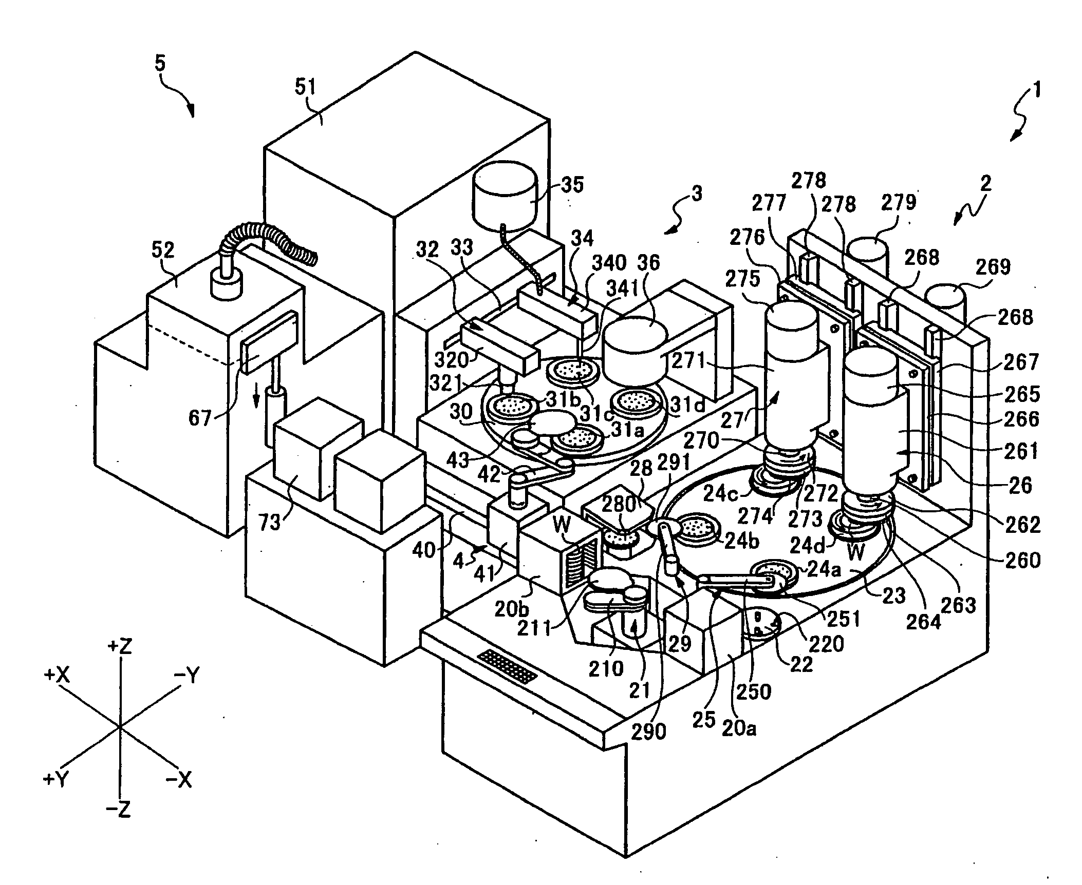
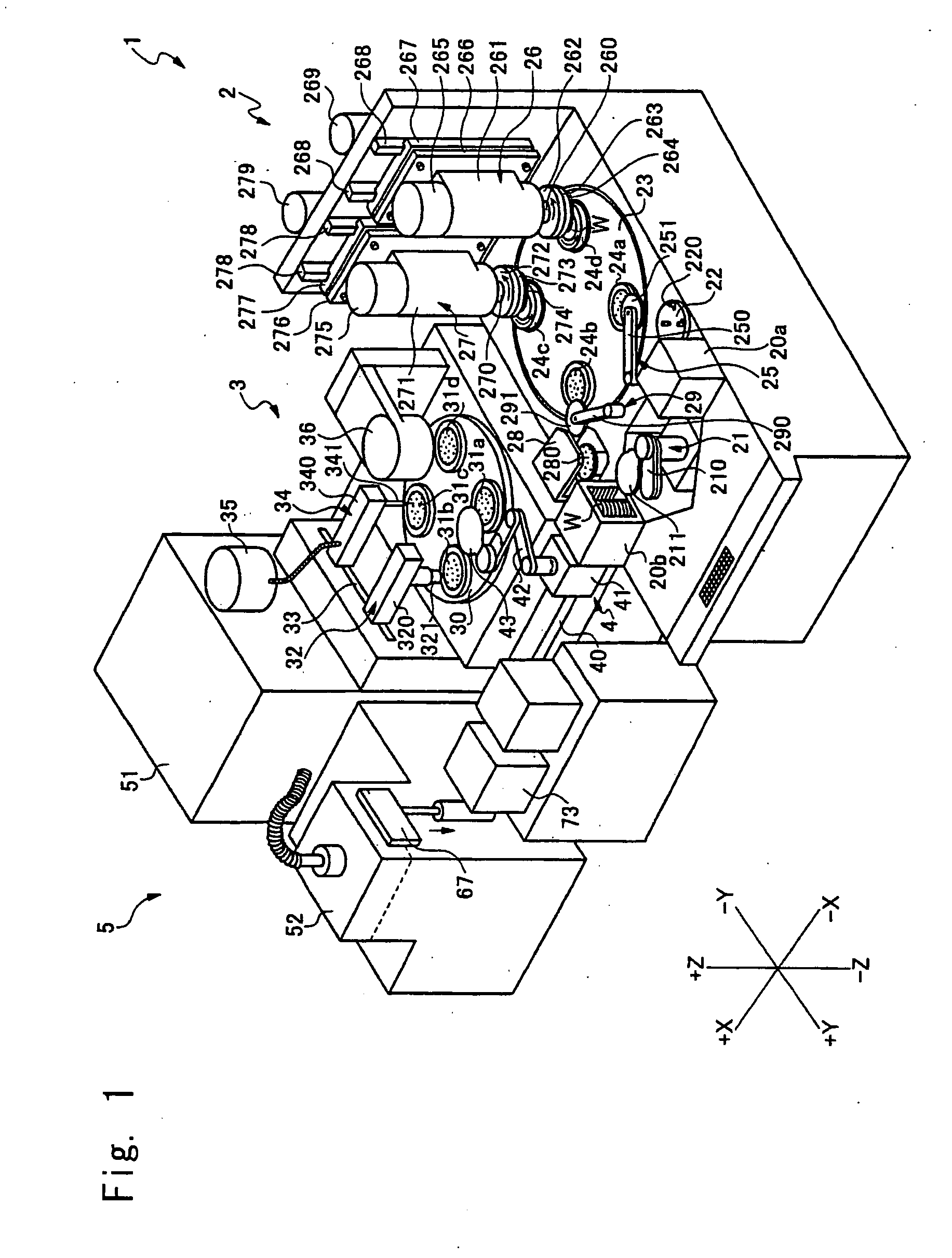
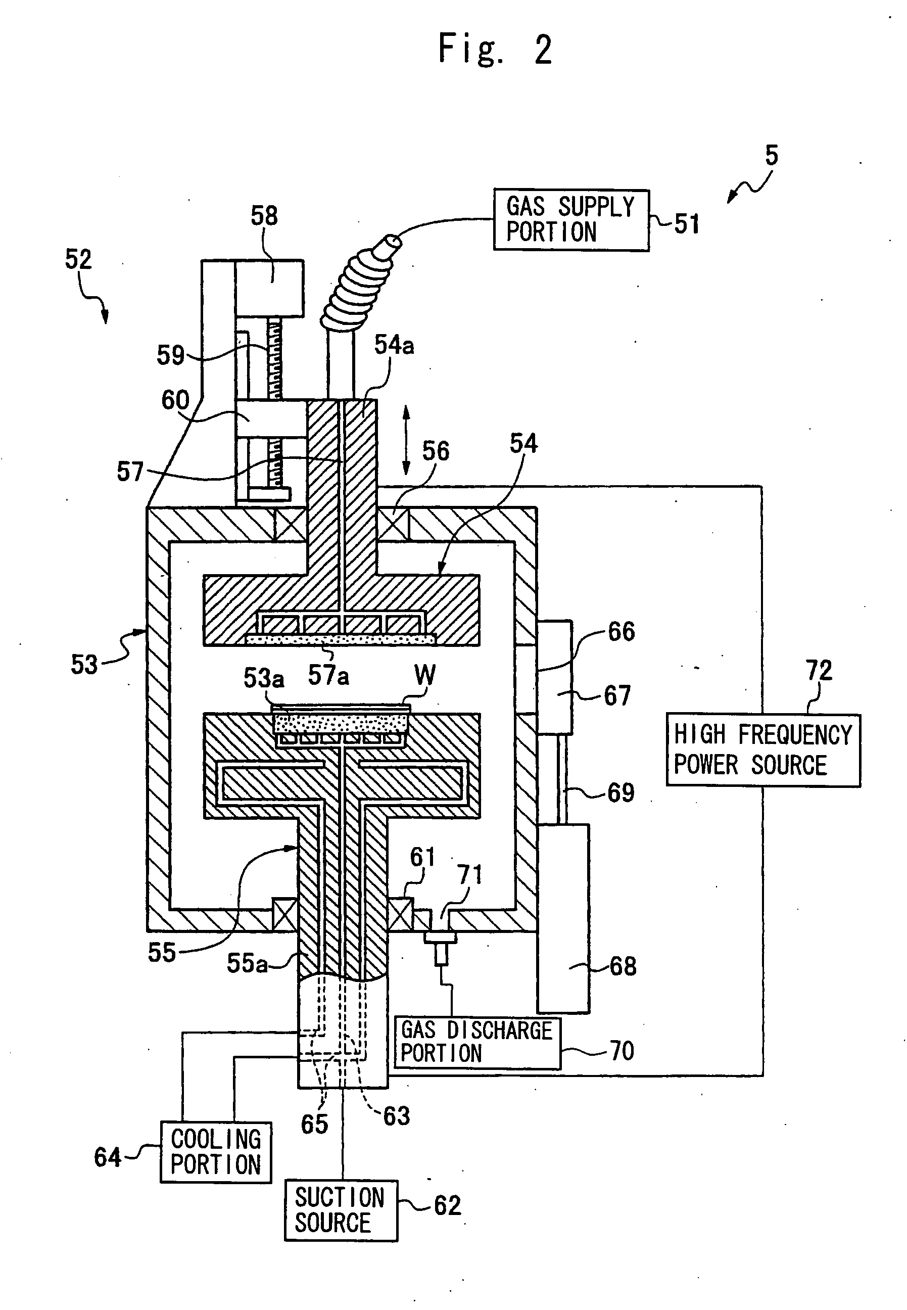
[0020] A wafer machining apparatus 1 shown in FIG. 1 shows an embodiment of the present invention, which comprises a grinding means 2 for grinding the back of a wafer to form the wafer in a predetermined thickness, a resist film coating means 3 for coating the back of the wafer with a resist film, and a plasma etching means 5 for dividing the wafer into individual devices by chemical etching.

[0021] The grinding means 2 is furnished with a first wafer cassette 20a and a second wafer cassette 20b for accommodating a plurality of wafers in a stacked state, and the wafers before grinding are accommodated into the first wafer cassette 20a and the second wafer cassette 20b.

[0022] A carry-out and carry-in means 21 having the function of carrying the wafer into and out of the necessary members is disposed between the first wafer cassette 20a and the second wafer cassette 20b. The carry-out and carry-in means 21 has a holding plate 211 provided at the front end of an arm portion 210 capabl...


PUM

PropertyMeasurementUnit
Adhesion strengthaaaaaaaaaa
Efficiencyaaaaaaaaaa

Abstract

The present invention provides a wafer machining apparatus which can separate streets with high efficiency, without deteriorating the quality of devices, in dividing a wafer into individual devices. The wafer machining apparatus comprises grinding means for grinding the back of the wafer; resist film coating means for passing a radiation from the back side to the face side of the wafer to recognize the streets, and coating a resist film onto regions other than street-corresponding regions; and plasma etching means for etching away the street-corresponding regions in a range from the back to the face of the wafer to divide the wafer into individual devices, and thus can perform a procedure ranging from grinding of the back of the wafer to the division of the wafer into the devices. In the resist film coating means, the wafer is imaged from the back side by an infrared imaging portion to recognize the streets formed on the face side, and a liquid resist is jetted from a resist jetting portion toward the regions other than the street-corresponding regions, whereby only the street-corresponding regions can be exposed.

Description

TECHNICAL FIELD [0001] This invention relates to a wafer machining apparatus having the function of etching streets formed in a wafer to divide the wafer into individual devices. BACKGROUND ART [0002] A wafer, on whose face a plurality of devices each composed of IC or LSI are formed by being partitioned by streets formed longitudinally and transversely, is divided into individual devices by separating the streets. The resulting devices are used in various types of electronic equipment. [0003] Usually, the streets are cut by a cutting blade rotating at a high speed. If the thickness of the wafer is as small as 100 μm or less or 50 μm or less, the problem occurs that the devices are chipped by the crushing force of the cutting blade, and their deflective strength decreases, deteriorating their quality. [0004] Thus, the following techniques have been proposed: A mask member is coated on the face of the wafer, and the cutting blade rotating at a high speed is cut into only portions of ...

Claims


Application Information

Patent Timeline
IPC IPC(8): H01L21/306C23F1/00
CPCH01L21/67092H01L21/67219H01L21/6835H01L21/78H01L2221/6834
Inventor FUJISAWA, SHINICHIONO, TAKASHI
Owner DISCO CORP
Why Eureka
Try Eureka