
Non-volatile transistor memory array incorporating read-only elements with single mask set

a memory array and non-volatile technology, applied in the direction of transistors, semiconductor devices, electrical equipment, etc., can solve the problem of the same footprint for all transistors in the memory array, and achieve the effect of greater geometric regularity in the array topology, greater functionality, and the same footprin

Inactive Publication Date: 2006-06-22
ATMEL CORP
View PDF9 Cites 2 Cited by
  • Summary
  • Abstract
  • Description
  • Claims
  • Application Information

AI Technical Summary

Benefits of technology

The present invention relates to a method for programming a non-volatile transistor memory element, specifically an EEPROM cell. The invention makes use of a mask that is used to define the areas within the cell that receive the implant. The mask is modified to provide programming data to the ROM cell. The invention allows the same EEPROM mask set to be used as a ROM mask of the same footprint on a selected basis, without any redesign of the existing microcircuit mask set or even the EEPROM mask set itself, or the manufacturing process. The technical effect of the invention is greater geometric regularity in the array topology and the opportunity to achieve greater functionality in a memory array that has the same dimensions as one without the enhanced functionality.

Problems solved by technology

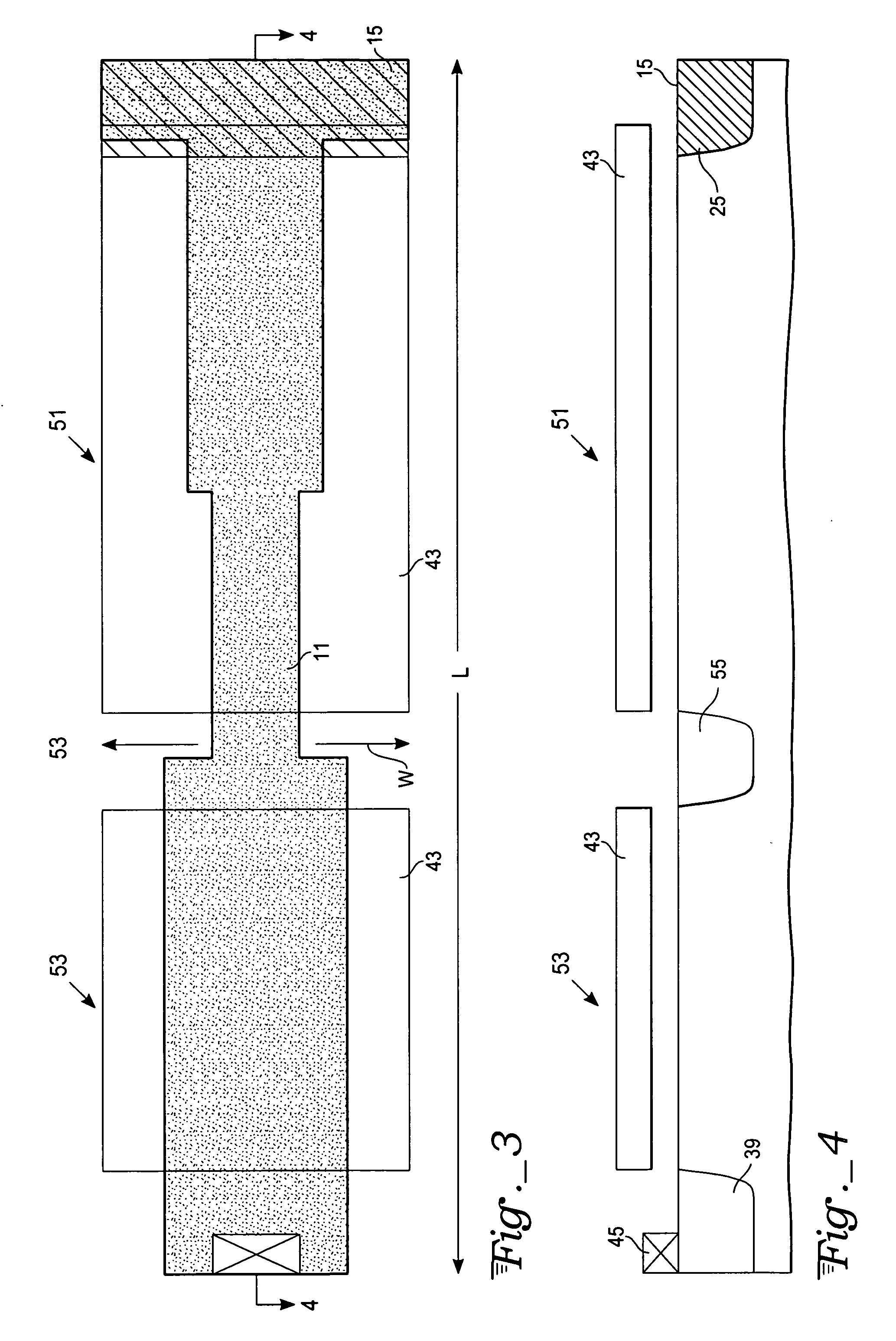
In other words, essentially the same set of masks can be used to form all transistors, both non-volatile memory elements and read-only memory elements with blocking or non-use on the one hand or opening of some mask portions on the other hand, thereby leading to the same footprint for all transistors in a memory array.

Method used


Image

  • Non-volatile transistor memory array incorporating read-only elements with single mask set
  • Non-volatile transistor memory array incorporating read-only elements with single mask set
  • Non-volatile transistor memory array incorporating read-only elements with single mask set

Examples


Embodiment Construction

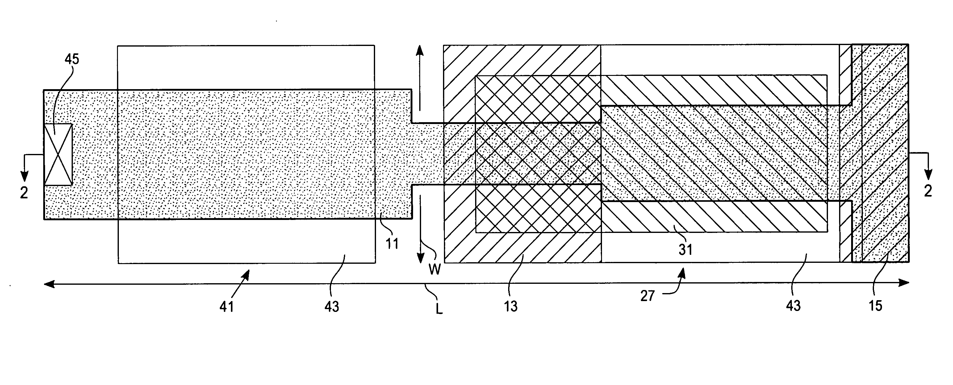
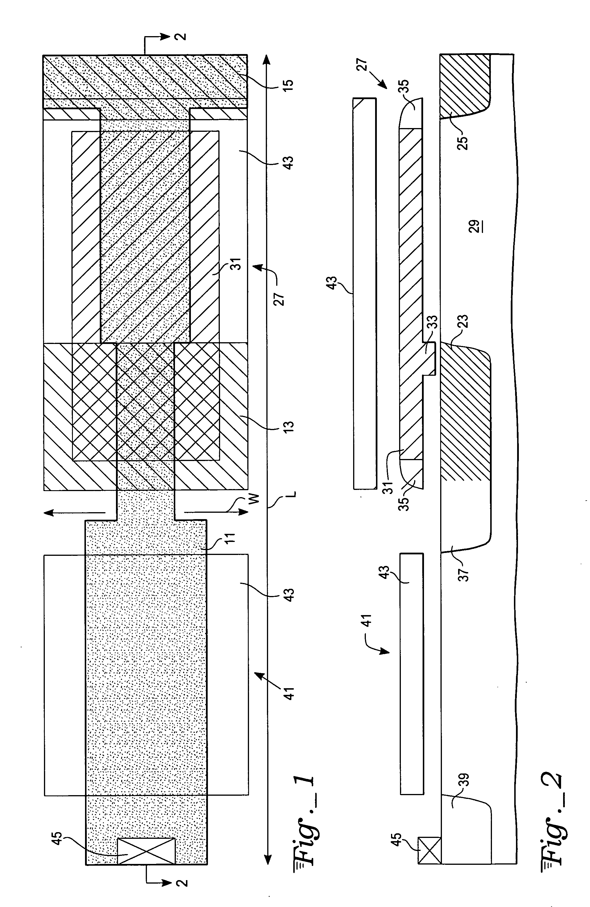
[0014] With reference to FIGS. 1 and 2, an EEPROM cell is shown having length L and width W dimensions, with an areawise footprint L×W. Such a cell would normally be a single element in an memory array having “n” rows and “m” columns where “n” and “m” are integers.

[0015] A p-type wafer has memory cells that are laid out by first establishing an active area 11, indicated by stippling in FIG. 1 and defined by a mask. The active area is seen to have longitudinal or lengthwise axis, parallel to line L, but running through the entire length of the active area. The active area is lightly doped and will contain source and drain implants for two MOS transistors.

[0016] Next, a buried n-diffusion is established in regions 13 and 15, indicated by forward-slant hatching. This is a heavily doped n+region in the substrate 29 suitable for forming electrodes. Region 13 forms part of drain 23 in FIG. 2 and n-diffusion region 15 forms part of source 25 in an EEPROM transistor 27. Between the subsur...


PUM


Abstract

A memory array has memory elements of identical topology or footprint arranged in rows and columns. Some of the memory elements are EEPROM cells and other memory elements are read only memory cells but all are made using a mask set having the same length and width dimensions. In the mask set for EEPROMs a principal mask is used for formation of a depletion implant. In the case of one type of read-only memory element, this mask is mainly blocked, leading to formation of a transistor with a non-conductive channel between source and drain. In the case of another read only memory element, the same mask is unblocked, leading to formation of a transistor with a highly conductive or almost shorted channel between source and drain. These two read only memory elements are designated as logic one and logic zero. By having rows of read-only memory elements with rows of EEPROMs on the same chip, a more versatile memory array chip may be built without sacrificing chip space.

Description

CROSS-REFERENCE TO RELATED APPLICATION [0001] This is a divisional of pending U.S. patent application Ser. No. 10 / 810,035 filed Mar. 26, 2004.TECHNICAL FIELD [0002] The invention relates to manufacturing a semiconductor memory array having non-volatile and read only memory devices. BACKGROUND ART [0003] Many complex microcircuits, especially those employing internal microcontrollers, have a need for non-volatile memory in which to store critical data. Typically this data consists of operating instructions for a microcontroller, although it may also consist of other critical data such as keys or configuration data. The development of this data is frequently a lengthy task, with the data not fully debugged until after a microcircuit is developed. Once this data is fully developed, it is often desirable to make the data permanent. There are several reasons for this. A first reason is that the overall security of the system may be compromised if the data can be altered. Another reason r...

Claims


Application Information

Patent Timeline
Patent Type & Authority Applications(United States)
IPC IPC(8): H01L29/94H01L21/8247H01L27/02H01L31/108H01L31/119H10B10/00H10B20/00H10B69/00
CPCH01L27/0207H01L27/105H01L27/112H01L27/11286H01L27/115H01L27/11517H01L27/11526H10B20/60H10B20/00H10B41/00H10B41/40H10B69/00
Inventor WEINER, ALBERT S.
Owner ATMEL CORP
Learn More