Semiconductor integrated circuit for liquid crystal display driver

a liquid crystal display and integrated circuit technology, applied in the direction of static indicating devices, non-linear optics, instruments, etc., can solve the problems of difficulty in reducing the size and cost of each tft liquid crystal display, and achieve the reduction of chip size and cost, the power consumption of the boosting circuit can be reduced, and the cost of the chip.

Inactive Publication Date: 2006-06-22
RENESAS TECH CORP
View PDF12 Cites 46 Cited by
  • Summary
  • Abstract
  • Description
  • Claims
  • Application Information

AI Technical Summary

Benefits of technology

[0017] According to the invention, in the liquid crystal drive controller having therein a power source circuit including a boosting circuit and formed as a semiconductor integrated circuit for driving a source line and a gate line of a TFT liquid crystal panel, by decreasing the number of external capacitive elements and the number of external terminals for connecting the...

Problems solved by technology

There is a problem such that it is difficult to reduce the size and cost of each of a TFT liquid crystal display (hereinbelow, called a TFT liquid crystal panel), a semicond...

Method used


Image

  • Semiconductor integrated circuit for liquid crystal display driver
  • Semiconductor integrated circuit for liquid crystal display driver
  • Semiconductor integrated circuit for liquid crystal display driver

Examples


third embodiment

[0066]FIGS. 11A and 11B show the boosting circuit according to the invention.

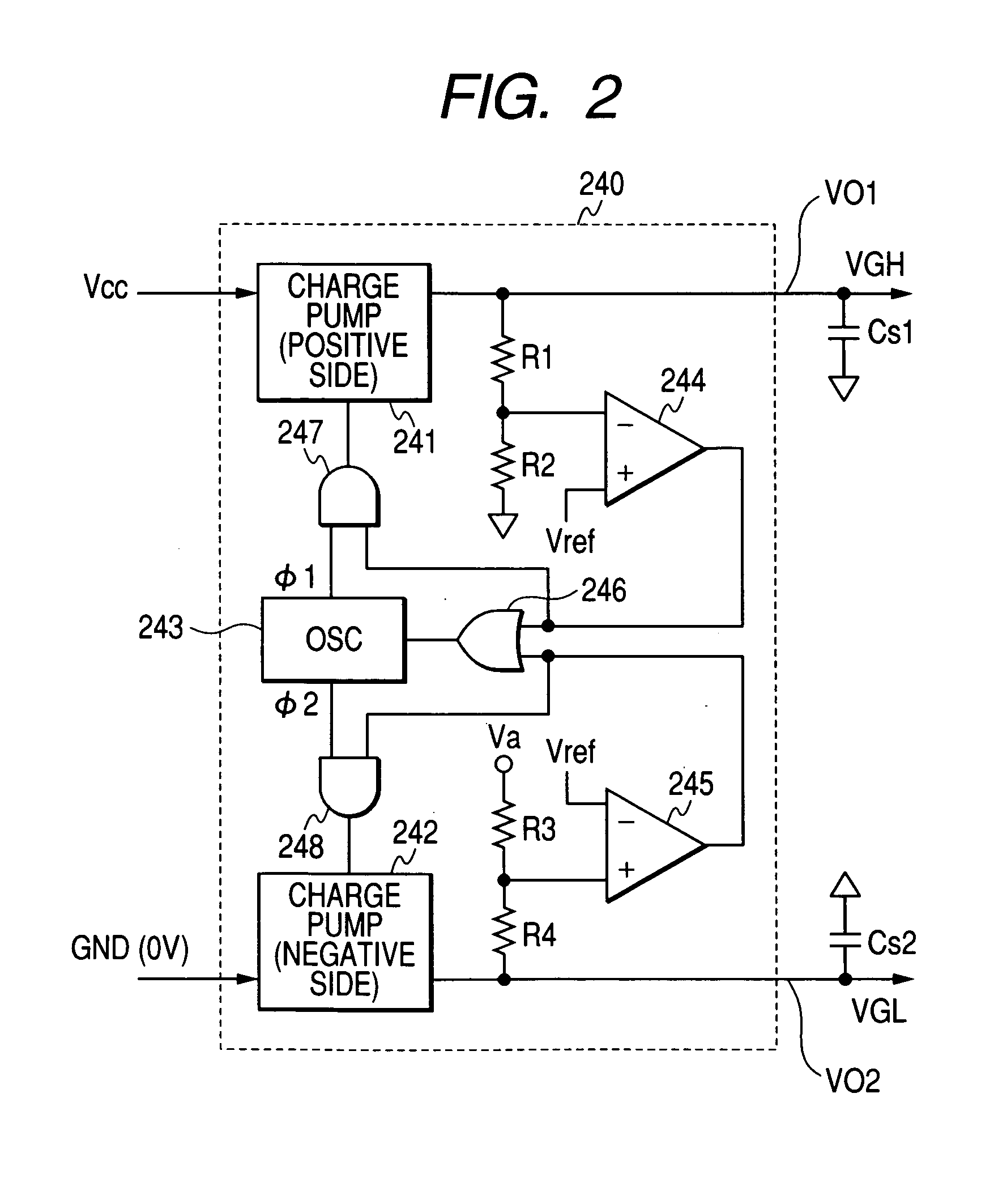
[0067] In the third embodiment, as shown in FIG. 11A, by using a variable resistor for one of resistors in each of the resistance dividing circuit constructed by the resistors R1 and R2 and the resistance dividing circuit constructed by the resistors R3 and R4 on the input side of the comparators 244 and 245 in the booster power source circuit 240 for the gate driver of the first embodiment shown in FIG. 2, the levels of the output boosting voltages VGH and VGL can be adjusted. By using variable resistors as the resistors R2 and R3 on the side opposite to the output node of VGH and VGL in the resistors R1 and R2 constructing the resistance dividing circuit and the resistors R3 and R4 constructing the resistance dividing circuit, low-withstand-voltage MOS transistors can be used as resistance switching elements.

[0068] Concretely, as shown in FIG. 11B, the voltage adjusting circuit is constructed by a plural...

fourth embodiment

[0070]FIG. 12 shows the boosting circuit according to the invention.

[0071] In the fourth embodiment, the number of boosting stages of the charge pumps 241 and 242 constructing the booster power source circuit 240 for the gate driver is made changeable, and is switched by a set value in a register REG2. In the fourth embodiment, for example, the set value of the register REG2 is changed in accordance with specifications of the liquid crystal panel, the display mode, or the operation mode. By switching the number of boosting stages of the charge pumps in accordance with a necessary boosting voltage value, wasted power consumption of the charge pumps can be reduced.

[0072] In the case of using a conventional charge pump in which a plurality of diode-connected MOS transistors are connected in series for switching the number of boosting stages of the charge pump, by providing a gate capable of supplying / interrupting a clock to each capacitor for boosting and controlling the number of gat...


PUM


Abstract

In a liquid crystal drive controller formed as a semiconductor integrated circuit having therein a power source circuit including a boosting circuit and driving a source line and a gate line of a TFT liquid crystal panel, the number of external capacitive elements and the number of external terminals for connecting the external capacitive elements are reduced, thereby reducing the size and cost of the chip and an electronic device on which the chip is mounted. As a boosting circuit for generating a voltage for driving a source line of the TFT liquid crystal panel in the liquid crystal controller having therein the power source including the boosting circuit, a boosting circuit having an external capacitive element is used. On the other hand, as a boosting circuit for generating a voltage for driving a gate line, a charge pump having a built-in (on-chip) capacitive element is used.

Description

CROSS-REFERENCE TO RELATED APPLICATION [0001] The present application claims priority from Japanese patent application No. 2004-368708 filed on Dec. 21, 2004, the content of which is hereby incorporated by reference into this application. BACKGROUND OF THE INVENTION [0002] The present invention relates to a semiconductor integrated circuit for a liquid crystal display driver having therein a booster power source circuit for generating a voltage obtained by boosting a power source voltage and, to a technique effective when used for an LSI (Large Scale Integration circuit) for controlling liquid crystal display having therein a liquid crystal driving power source circuit for driving, for example, a TFT (Thin Film Transistor) liquid crystal display. [0003] In recent years, as a display of a portable electronic device such as a cellular phone or PDA (Personal Digital Assistants), a dot-matrix liquid crystal panel in which a plurality of display pixels are arranged two-dimensionally in a...

Claims


Application Information

Patent Timeline
IPC IPC(8): G09G3/36
CPCG09G3/3674G09G3/3685G09G3/3696G02F1/133
Inventor SHIGENOBU, TAKESHIHIRAKI, MITSURUHORIGUCHI, MASASHIOKADO, KAZUOAKIBA, TAKESADA
Owner RENESAS TECH CORP
Why Eureka
Try Eureka