Arrayed waveguide wavelength multiplexing apparatus and optical transmitter

a wavelength multiplexing and waveguide technology, applied in the direction of optical waveguide light guides, instruments, optical elements, etc., can solve the problems of deterioration of optical signal characteristics, side lobe crosstalk deterioration, dampening, etc., to increase the density of individual hardware components, promote cost reduction, and expand the utilization of wavelength division multiplexing

Inactive Publication Date: 2006-01-10
FUJITSU LTD
View PDF16 Cites 5 Cited by
  • Summary
  • Abstract
  • Description
  • Claims
  • Application Information

AI Technical Summary

Benefits of technology

[0048]The present invention has been conceived in view of the above-described problems and aims at providing an arrayed waveguide wavelength division multiplexing apparatus and an optical transmitter, which have a highly desirable waveguide characteristic, such as a reduction in chip size and a reduction in costs of a chip, in connection with a wavelength division multiplexing apparatus used in, e.g., wavelength division multiplexing or optical signal processing.
[0050]Consequently, by virtue of this, the chip size of the arrayed waveguide wavelength division multiplexing apparatus can be reduced. As a result, the chip size is reduced, and the number of chips per unit wafer is increased, thereby curtailing costs of the chip.
[0051]Moreover, the first or second neighborhood of at least one of the plurality of channel waveguides may be formed so as to bend in a direction from a center channel waveguide of the plurality of channel waveguides to an outer channel waveguide. Alternatively, the first or second neighborhood of at least one of the plurality of channel waveguides may be formed from a plurality of waveguide shaving geometries of different degrees of flex for the respective channel waveguides. By virtue of this, miniaturization of the chip size is promoted, and efficiency of mass production is significantly enhanced.
[0055]Accordingly, by means of this configuration, there can be obtained a compact arrayed wavelength division multiplexing apparatus without involvement of deterioration of characteristics, which would otherwise be induced by coupling between the channel waveguides in an area other than the slab connection section.
[0057]Further, curvature radii of respective S-shaped waveguides serving as the plurality of channel waveguides may be made smaller from a center waveguide of the input or output waveguides toward an outer waveguide. Alternatively, curvature radii of respective S-shaped waveguides serving as the plurality of channel waveguides may be made smaller from a shortest channel waveguide toward a longest channel waveguide of the input or output waveguides. By means of these configurations, a loss in a waveguide and a loss in the slab connection section can be diminished by reducing a chip size. Thereby, utilization of wavelength division multiplexing is expanded.
[0060]Accordingly, by means of this configuration, the packing density of individual hardware components is increased by miniaturization, thereby promoting cost reduction and expanding utilization of wavelength division multiplexing.

Problems solved by technology

Thereby, an error between the amounts of changes in phases of the light waves traveling through the arrayed waveguide becomes small, and crosstalk deterioration due to a side lobe, or the like, is dampened.
(1-4) However, signal lights (separated light) propagating through the respective channel waveguides “a” to “g” of the AWG all shift to any of the adjacent channel waveguides “a” to “g” while propagating through the channel waveguides “a” to “g,” whereby distortion of phase information (phase difference) and deteriorating characteristics of respective signal lights are induced, to thus cause so-called crosstalk.
As mentioned above, when the adjacent channel waveguides are arranged over a long distance while being separated from each other by only a small interval d1, the adjacent channel waveguides cause cross-talk or a transmission loss, thereby deteriorating characteristics of an optical signal.
Therefore, there exists a problem of an increase in the slab length f1 or f′ and an increase in the chip size of the AWG.

Method used


Image

  • Arrayed waveguide wavelength multiplexing apparatus and optical transmitter
  • Arrayed waveguide wavelength multiplexing apparatus and optical transmitter
  • Arrayed waveguide wavelength multiplexing apparatus and optical transmitter

Examples


first embodiment

[0081](A) Description of the Present Invention

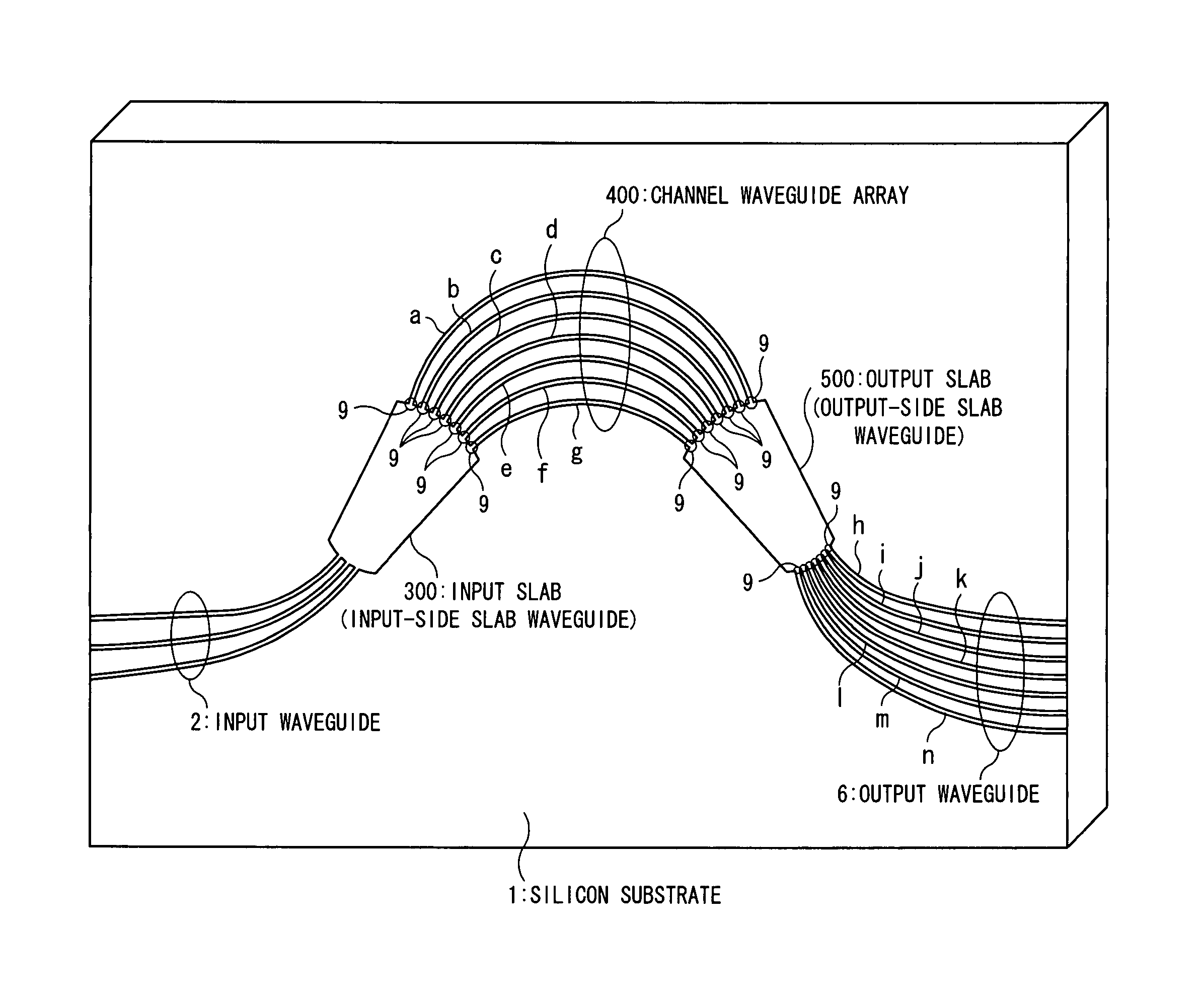
[0082]FIG. 1 is a block diagram of an AWG according to a first embodiment of the present invention. An AWG 1 shown in FIG. 1 can realize a multiplexing function as a wavelength multiplexer for multiplexing optical signals of different wavelengths and a wavelength division function as a wavelength divider for dividing multiplexed light into optical signals of different wavelengths. The AWG comprises a substrate 1 (AWG 1), and optical waveguides collectively fabricated on the substrate 1 through use of photolithography. The AWG has an input waveguide 2, an input slab (an input-side slab waveguide) 3, an arrayed waveguide (a channel waveguide array) 4 formed from six channel waveguide groups “a” to “f,” an output slab (an output-side slab waveguide) 5, and an output waveguide 6 formed from six waveguides “h” to “l” (el).

[0083]Here, wavelength-multiplexed lights #1 to #6 are transmitted in a direction from the input waveguide 2 toward the ou...

second embodiment

[0158](B) Descriptions of the Present Invention

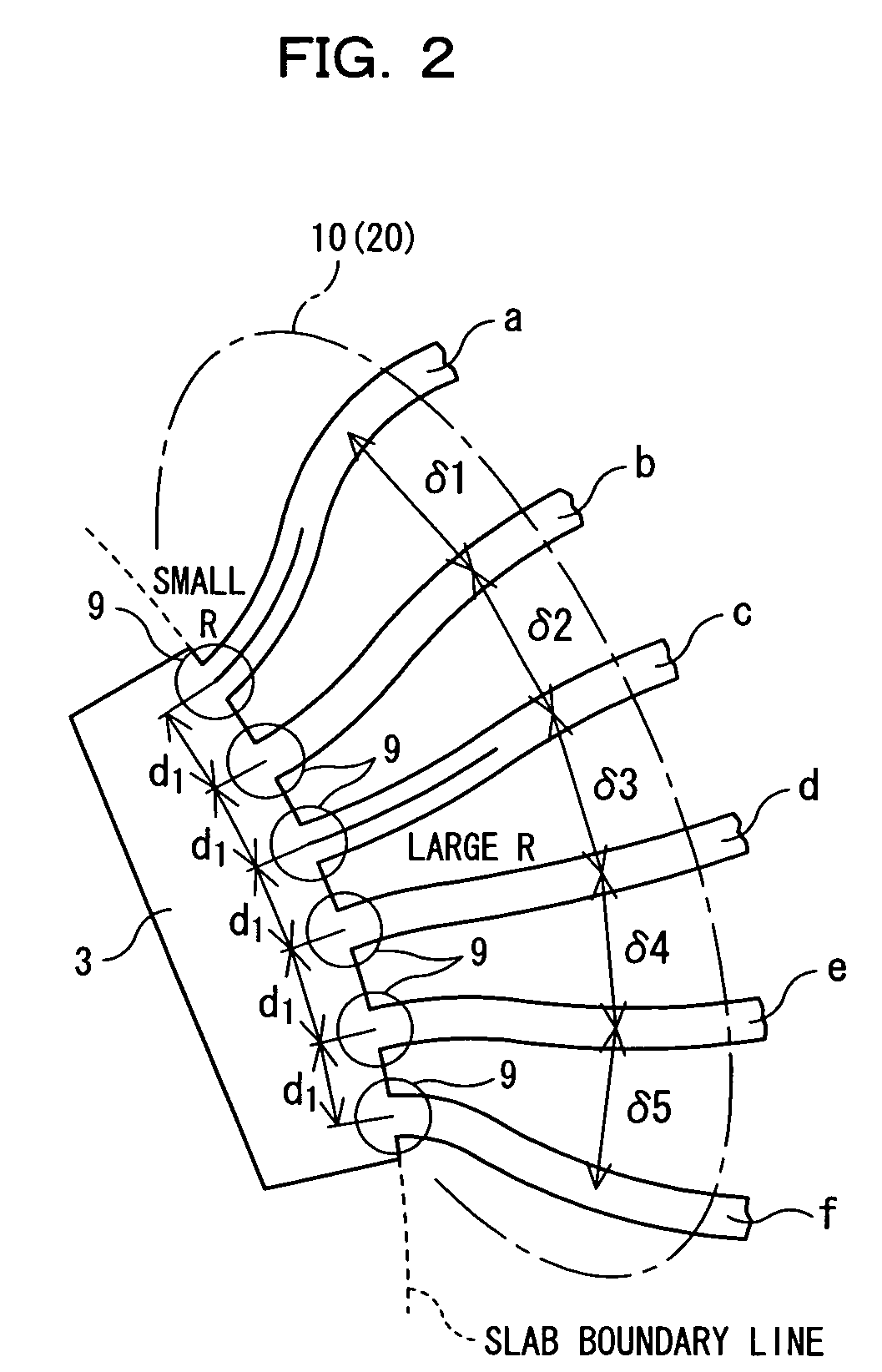
[0159]In the first embodiment, the locations where the S-shaped waveguides 10, 20 are formed are in the vicinity of the areas of the channel waveguides “a” to “f” connected to the input slab 3. However, the areas may be changed. In the second embodiment, the S-shaped waveguide section is provided in the input waveguide 2 of the AWG.

[0160]FIG. 12 is a block diagram of an AWG according to the second embodiment. An AWG 1c shown in FIG. 12 is formed such that the channel waveguide interval d1 in the neighborhood of an area of the input waveguide 2 connected to the input slab 3 becomes wider than the channel waveguide interval d1 in the area of the input waveguide 2 connected to the input slab 3 (the third connection section). The AWG 1c is formed such that the channel waveguide interval d1 in the neighborhood of an area of the output waveguide 6 connected to the output slab 5 becomes wider than the channel waveguide interval d1 in the area ...


PUM


Abstract

For a WDM optical communication, on a substrate of an arrayed waveguide type wavelength multiplexing / demultiplexing device, input waveguide propagates a plurality of light and outputs WDM light; a first slab diffuses the WDM light outputted from the input waveguide; a channel waveguide array separates the WDM light and causes the separated six lights to propagate; a second slab condenses the separated six lights having propagated through the channel waveguide array; output waveguides causes the separated six lights condensed to propagate, and a waveguide interval in first neighborhoods connected to the first slab is set to become wider than a first waveguide interval in a first connection section for connecting the channel waveguide array to the first slab, which achieves a reduced chip size, cost-reduction of chips, and reduces loss.

Description

[0001]This application is a continuation application, filed under 35 USC 111(a), of International Application PCT / JP2003 / 002124, filed Feb. 26, 2003.FIELD OF THE INVENTION[0002]The present invention relates to an arrayed waveguide wavelength multiplexing apparatus and an optical transmitter, which are suitable for use with a waveguide integrated optical component; e.g., wavelength division multiplexing or optical signal processing.BACKGROUND[0003](1) In wavelength division multiplexing (WDM) for simultaneously transmitting a plurality of optical signals of different wavelengths, a wavelength division multiplexing apparatus is an important device. A wavelength division multiplexing apparatus has the function of a wavelength multiplexing apparatus for multiplexing optical signals of different wavelengths (a multiplexing function) and the function of a wavelength divider for dividing wavelength-multiplexed light into optical signals of different wavelengths (a wavelength division funct...

Claims


Application Information

Patent Timeline
Patent Type & Authority Patents(United States)
IPC IPC(8): G02B6/00G02B6/36G02B6/34
CPCG02B6/12011G02B6/12
Inventor NAKAGAWA, GOJI
Owner FUJITSU LTD
Why Eureka
Try Eureka