Flip-chip bonding structure of light-emitting element using metal column

a technology of light-emitting elements and metal columns, which is applied in the direction of lasers, semiconductor lasers, solid-state devices, etc., can solve the problems of reduced heat emission efficiency, and severe problems such as low thermal conductivity of solder bumps, and achieve large thermal conductivity and improve heat emission efficiency

Inactive Publication Date: 2006-06-29
SAMSUNG ELECTRO MECHANICS CO LTD
View PDF2 Cites 12 Cited by
  • Summary
  • Abstract
  • Description
  • Claims
  • Application Information

AI Technical Summary

Benefits of technology

[0011] The present invention may provide a flip-chip bonding structure of a light-emitting element capable of improving the heat emission efficiency by using a metal column of a large thermal conductivity instead of a solder bump.

Problems solved by technology

In a bonding structure of a related art that uses the solder bump, the low thermal conductivity of the solder bump is problematic.
Therefore, in when bonding using a solder bump, the thermal conductivity is gradually increased along a heat emission path from a heat source to the final heat emission point, so that the heat emission efficiency is diminished.
Recently, as heat generation is increased and the temperature is raised due to the high power trend of the light-emitting elements such as semiconductor laser diode, the low thermal conductivity of the solder bump emerges as a severe problem.

Method used


Image

  • Flip-chip bonding structure of light-emitting element using metal column
  • Flip-chip bonding structure of light-emitting element using metal column
  • Flip-chip bonding structure of light-emitting element using metal column

Examples


Embodiment Construction

[0028] The present invention will now be described more fully with reference to the accompanying drawings, in which exemplary embodiments of the invention are shown. The invention may, however, be embodied in many different forms and should not be construed as being limited to the embodiments set forth herein.

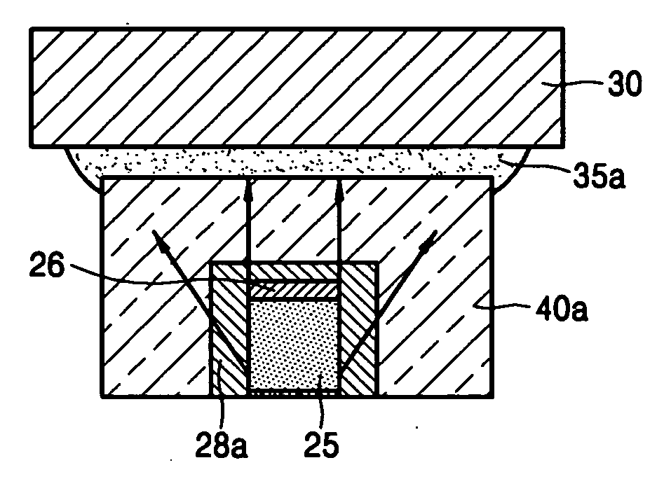
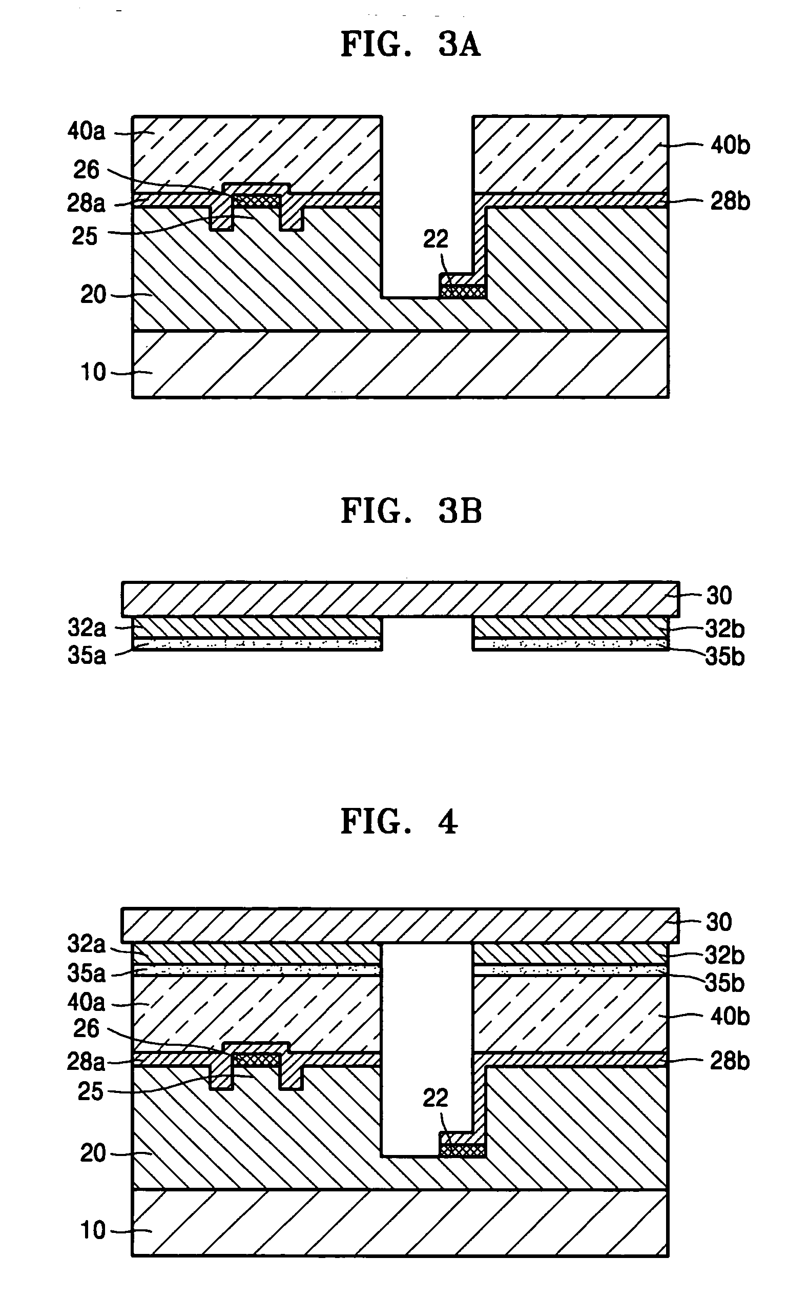
[0029]FIGS. 3A and 3B are cross-sectional views illustrating a light-emitting element portion and a sub-mount portion in a flip-chip bonding structure of a light-emitting element according to the present invention.

[0030] First, referring to FIG. 3A, first and second metal pad layers 28a and 28b are formed respectively on a light-emitting element 20 formed on a sapphire substrate 10. Metal columns 40a and 40b are formed respectively on the first and the second metal pad layers 28a and 28b. The light-emitting element 20 exemplarily shown in FIG. 3A is an edge-emitting type semiconductor laser device, where a laser beam is emitted in a direction perpendicular to the drawing from...


PUM

PropertyMeasurementUnit
thicknessaaaaaaaaaa
thicknessesaaaaaaaaaa
temperatureaaaaaaaaaa

Abstract

A flip-chip bonding structure of a light-emitting element is provided. The structure improves a heat emission efficiency by using a metal column having a high thermal conductivity instead of a solder bump. The structure includes a light-emitting element, a sub-mount, and a metal column. The metal column connects the light-emitting element with the sub-mount electrically and thermally.

Description

CROSS-REFERENCE TO RELATED PATENT APPLICATION [0001] This application claims the benefit of Korean Patent Application No. 10-2004-0115070, filed on Dec. 29, 2004, in the Korean Intellectual Property Office, the disclosure of which is incorporated herein in its entirety by reference. BACKGROUND OF THE DISCLOSURE [0002] 1. Field of the Disclosure The disclosure relates to a flip-chip bonding structure of a light-emitting element using a metal column, and more particularly, to a flip-chip bonding structure of a light-emitting element capable of improving the heat emission efficiency by using a metal column of a large thermal conductivity instead of a solder bump. [0003] 2. Description of the Related Art [0004] As illustrated in FIG. 1, a wire-bonding has been primarily used in bonding light-emitting elements such as a laser diode (LD) or a light-emitting diode (LED) to a package. That is, an operation current and voltage are applied by connecting both ends of wires 150a and 150b to res...

Claims


Application Information

Patent Timeline
Patent Type & Authority Applications(United States)
IPC IPC(8): H01L29/24H01L33/64H01L33/62H01S5/023H01S5/0233
CPCH01L33/62H01L33/641H01L33/647H01S5/02236H01S5/0224H01S5/02256H01S5/02272H01S5/02476H01S5/0425H01L2224/48091H01L2924/00014H01S5/04254H01S5/04252H01S5/04257H01S5/02355H01S5/0237H01S5/0234H01S5/023H01S5/0233H01S5/0235
Inventor CHIO, WON-KYOUNGJANG, TAE-HOONCHAE, SU-HEEKIM, HYUNG-KUN
Owner SAMSUNG ELECTRO MECHANICS CO LTD
Why Eureka
Try Eureka