CMOS image sensor and method for fabricating the same

a metal oxidesemiconductor and image sensor technology, applied in the direction of diodes, radiation control devices, semiconductor devices, etc., can solve the problem that the gate is usually partially exposed, and achieve the effect of enhancing transistor uniformity, facilitating electron mobility, and improving transfer characteristics

Inactive Publication Date: 2006-06-29
DONGBU ELECTRONICS CO LTD
View PDF3 Cites 24 Cited by
  • Summary
  • Abstract
  • Description
  • Claims
  • Application Information

AI Technical Summary

Benefits of technology

[0009] An advantage of the present invention is to provide a CMOS image sensor and a method for fabricating the same which facilitates electron mobility.
[0010] Another advantage of the present invention is to provide a CMOS image sensor and a method for fabricating the same which obtains improved transfer characteristics.
[0011] Another advantage of the present invention is to provide a CMOS image sensor and a method for fabricating the same which prevents an ion-plantation process for forming a photodiode from adversely affecting a channel region.
[0012] Another advantage of the present invention is to provide a CMOS image sensor and a method for fabricating the same which enhances transistor uniformity across a pixel array and promotes higher yields.
[0013] Additional features and advantages of the invention will be set forth in the description which follows, and in part will be apparent from the description, or may be learned by practice of the invention. The objectives and other advantages of the invention will be realized and attained by the structure and method particularly pointed out in the written description and claims hereof as well as the appended drawings.
[0014] To achieve these and other advantages and in accordance with the purpose of the present invention, as embodied and broadly described, there is provided a CMOS image sensor comprising a semiconductor substrate having at least one active region defined by a shallow trench isolation region; a light-receiving region formed in a surface of the semiconductor substrate; and a transfer gate in the semiconductor substrate between the light-receiving region and the at least one active region, wherein the transfer gate has a trench shape of a predetermined depth.

Problems solved by technology

The gate, however, is usually partially exposed because of inherent inaccuracies in a photo-masking process of the ion implantation process.

Method used


Image

  • CMOS image sensor and method for fabricating the same
  • CMOS image sensor and method for fabricating the same
  • CMOS image sensor and method for fabricating the same

Examples


Embodiment Construction

[0021] Reference will now be made in detail to embodiments of the present invention, examples of which are illustrated in the accompanying drawings. Wherever possible, like reference designations will be used throughout the drawings to refer to the same or similar parts.

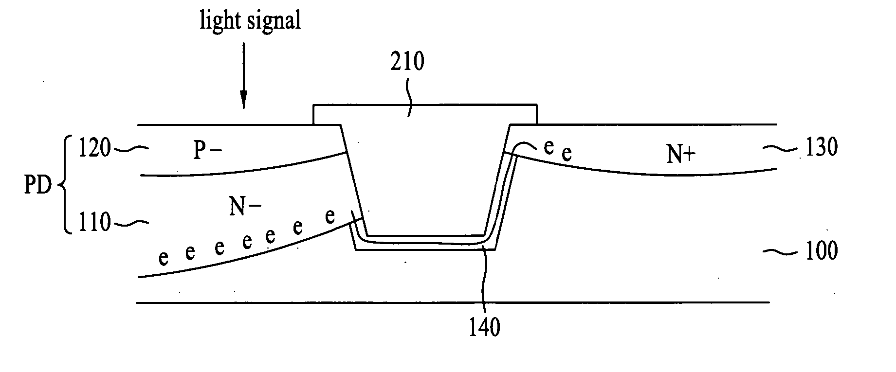
[0022] The CMOS image sensor is structured as an array of pixels, wherein each pixel is comprised of an arrangement of four transistors and a photodiode.

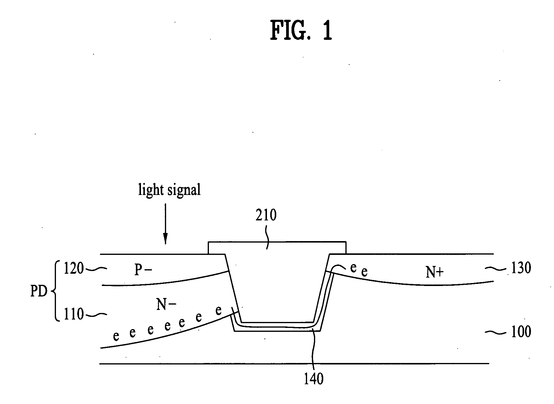
[0023] As shown in FIG. 1, a semiconductor or substrate or silicon substrate 100 of the CMOS image sensor according to the present invention includes a photodiode PD serving as a light-receiving region formed in a predetermined surface of the semiconductor substrate. An active region 130, which is preferably formed of polysilicon, is buried in the semiconductor substrate 100 in a trench shape. Thus, if a transfer gate 210 is turned on, a channel region 140 is formed deep inside the semiconductor substrate 100 to extend, below a trench, from the photodiode PD to the...


PUM


Abstract

A CMOS image sensor and a method for fabricating the same forms a trench-shaped transfer gate that serves to better transfer electrons generated by light incident on photodiodes, thus obtaining improved transfer characteristics. The CMOS image sensor includes a semiconductor substrate having at least one active region defined by a shallow trench isolation region; a light-receiving region formed in a surface of the semiconductor substrate; and a transfer gate buried in the semiconductor substrate between the light-receiving region and the at least one active region, wherein the transfer gate has a trench shape of a predetermined depth.

Description

[0001] This application claims the benefit of Korean Patent Application No. 10-2004-0111470, filed on Dec. 23, 2004, which is hereby incorporated by reference for all purposes as if fully set forth herein. BACKGROUND OF THE INVENTION [0002] 1. Field of the Invention [0003] The present invention relates to complementary metal-oxide-semiconductor (CMOS) image sensors and more particularly, to a CMOS image sensor and a method for fabricating the same, which employs a trench-shaped transfer gate that facilitates the transfer of electrons generated by light incident on a photodiode. [0004] 2. Discussion of the Related Art [0005] An image sensor is a semiconductor device for converting optical images to electrical signals and may be categorized as a CMOS image sensor or a charge-coupled device. A charge-coupled device includes a plurality of metal-oxide-silicon (MOS) capacitors arranged in proximity to one another, wherein charge carriers are stored in and transferred to the capacitors. A...

Claims


Application Information

Patent Timeline
Patent Type & Authority Applications(United States)
IPC IPC(8): H01L31/113
CPCH01L27/1463H01L27/14643H01L27/14689H01L27/146H01L27/14H01L31/10
Inventor LIM, KEUN HYUK
Owner DONGBU ELECTRONICS CO LTD
Why Eureka
Try Eureka