Manufacture method of low temperature poly-silicon TFT substrate and low temperature poly-silicon TFT substrate

a manufacturing method and technology of low temperature polysilicon tft, which are applied in the field of display technology, can solve the problems that the crystallization technology according to prior art cannot achieve effective control of the uniformity of the lattices and the crystallization direction of the lattices, and the display effect is not uniform, so as to raise the light uniformity of the oled, promote the electron, and raise the current. the effect of uniformity

Active Publication Date: 2018-02-22
WUHAN CHINA STAR OPTOELECTRONICS TECH CO LTD
View PDF3 Cites 0 Cited by
  • Summary
  • Abstract
  • Description
  • Claims
  • Application Information

AI Technical Summary

Benefits of technology

[0049]The benefits of the present invention are: in the manufacture method of the Low Temperature Poly-silicon TFT substrate and the Low Temperature Poly-silicon TFT substrate according to the present invention, by locating one heat sink layer under the amorphous silicon layer in advance, the difference of the crystallizations of the polysilicons in the drive area and the display area can exist after implementing an Excimer Laser Annealing process to the amorphous silicon layer, and in the drive area, the polysilicon with the larger lattice dimension is formed to promote the electron mobility; the fractured crystals can be achieved in the crystallization process of the display area to form the polysilicon with the smaller lattice dimension for ensuring the uniformity of the grain boundary and raising the uniformity of the current, and thus, the electrical property demands for the different TFTs can be satisfied to raise the light uniformity of the OLED.

Problems solved by technology

However, the ELA crystallization technology according to prior art cannot achieve effective control to the uniformity of the lattices and the crystallization direction of the lattices.
The distribution of crystallization condition in the entire substrate is extremely nonuniform and results in that the display effect is not uniform.

Method used


Image

  • Manufacture method of low temperature poly-silicon TFT substrate and low temperature poly-silicon TFT substrate
  • Manufacture method of low temperature poly-silicon TFT substrate and low temperature poly-silicon TFT substrate
  • Manufacture method of low temperature poly-silicon TFT substrate and low temperature poly-silicon TFT substrate

Examples


first embodiment

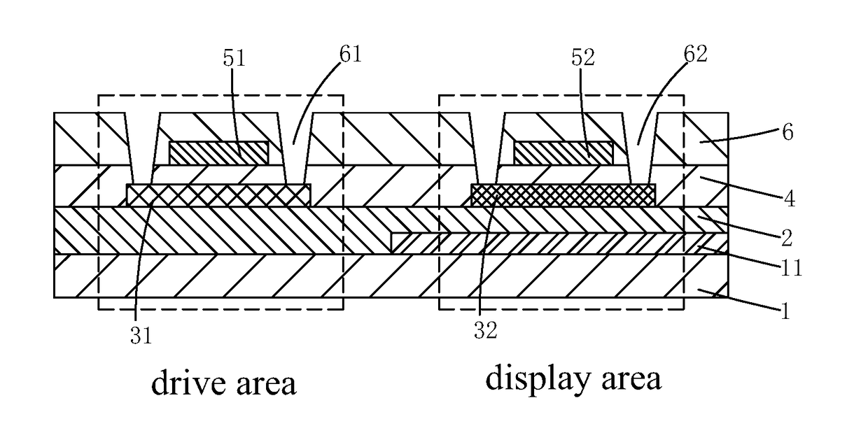
[0114]Please refer to FIG. 14, which is a sectional structure diagram of a Low Temperature Poly-silicon TFT substrate according to the present invention. In the display area, a heat sink section 11 is provided under the second polysilicon section 32 between the substrate 1 and the buffer layer 2, and material of the heat sink section 11 is metal, such as molybdenum (Mo), titanium (Ti), aluminum (Al) and copper (Cu).

second embodiment

[0115]Please refer to FIG. 24, which is a sectional structure diagram of a Low Temperature Poly-silicon TFT substrate according to the present invention. In the display area, a heat sink section 11 is provided under the second polysilicon section 32 between the buffer layer 2 and the second polysilicon section 32, and material of the heat sink section 11 is nonconducting metallic oxide, such as aluminum oxide.

[0116]Specifically, a lattice dimension of the first polysilicon section 31 is larger than a lattice dimension of the second polysilicon section 32.

[0117]Specifically, the substrate 1 is a glass substrate.

[0118]Specifically, material of the buffer layer 2, the gate isolation layer 4 and the interlayer insulation layer 6 is Silicon Nitride, Silicon Oxide or a combination of the two.

[0119]Specifically, material of the first gate 51, the second gate 52, the first source / the first drain 71 and the second source / the second drain 72 is a stack combination of one or more of molybdenum...


PUM

PropertyMeasurementUnit
Temperatureaaaaaaaaaa
lattice dimensionaaaaaaaaaa
brightnessaaaaaaaaaa

Abstract

The present invention provides a manufacture method of a Low Temperature Poly-silicon TFT substrate and a Low Temperature Poly-silicon TFT substrate, in which by locating one heat sink layer under the amorphous silicon layer in advance, the difference of the crystallizations of the polysilicons in the drive area and the display area can exist after implementing an Excimer Laser Annealing process to the amorphous silicon layer, and in the drive area, the polysilicon with the larger lattice dimension is formed to promote the electron mobility; the fractured crystals can be achieved in the crystallization process of the display area to form the polysilicon with the smaller lattice dimension for ensuring the uniformity of the grain boundary and raising the uniformity of the current, and thus, the electrical property demands for the different TFTs can be satisfied to raise the light uniformity of the OLED.

Description

FIELD OF THE INVENTION[0001]The present invention relates to a display technology field, and more particularly to a manufacture method of a Low Temperature Poly-silicon TFT substrate and a Low Temperature Poly-silicon TFT substrate.BACKGROUND OF THE INVENTION[0002]The Low Temperature Poly-silicon (LTPS) technology is the manufacture technology of the new generation TFT substrate. The response speed of the LTPS display is faster and possesses advantages of high brightness, high resolution and low electrical power consumption. The Poly-silicon (Poly-Si) possesses excellent electrical property, and the better drive ability to the Active-Matrix Organic Light Emitting Diode (AMOLED). Thus, the AMOLED display back plate based on the Low Temperature Poly-silicon technology has been widely utilized at present.[0003]The Excimer Laser Annealing (ELA) technology is the key skill in the LTPS manufacture process. The skill is to utilize the transient pulses of the laser to irradiate on the surfa...

Claims


Application Information

Patent Timeline
Patent Type & Authority Applications(United States)
IPC IPC(8): H01L29/66H01L21/265H01L29/786H01L27/085H01L27/32H01L21/77
CPCH01L29/66492H01L21/26506H01L29/78618H01L29/78672H01L27/085H01L27/3225H01L21/77H01L27/1203H01L27/1229H01L27/1281H01L2021/775H10K59/12H01L29/66757H01L27/1218H01L27/1285H10K59/00H01L27/12
Inventor ZHANG, ZHANDONGTANG, FUHSIUNG
Owner WUHAN CHINA STAR OPTOELECTRONICS TECH CO LTD
Why Eureka
Try Eureka