Current driver, data driver, display device and current driving method

a current driver and data driver technology, applied in the direction of pulse generators, pulse techniques, instruments, etc., can solve the problems of small variation in characteristics of transistors located close to each other, and the uniformity of output currents of current driving apparatuses, so as to reduce the circuit size of current drivers

Inactive Publication Date: 2006-06-29
GK BRIDGE 1
View PDF7 Cites 2 Cited by
  • Summary
  • Abstract
  • Description
  • Claims
  • Application Information

AI Technical Summary

Benefits of technology

[0045] In the inventive current driver, the current value of the output current flowing in the first driving transistor can be set to be a desired value in the first mode and the current value of the output current flowing in the second driving transistor can be set to be a desired value in the second mode. Suppose that a current driver (i.e., a current driver A) and a current driver (i.e., a current driver B) which are set to be the first mode and the second mode, respectively, and arranged adjacent to each other are used. Moreover, suppose that the first driving transistor provided in the current driver A and the second driving transistor provided in the current driver B are located close to each other. In such a case, if the current value of the output current flowing in the first driving transistor provided in the current driver A and the current value of the output current flowing in the second driving transistor provided in the current driver B are made to match each other, the current value of the output current from the current driver A and the current value of the output current from the current driver B can be made uniform (or to exhibit a certain slope). That is, there is no large difference among respective current values of output currents around a boundary line between the current driver A and the current driver B. Moreover, unlike the known current driver, a separate component(s) for adjusting a current value of an output current do not have to be provided in each of the first and second driving transistors. Therefore, a circuit size of a current driver can be reduced.
[0074] According to the inventive method, a current value of an output current flowing in the first driving transistor can be set to be a desired value in the first mode, and a current value of an output current flowing in the second driving transistor can be set to be a desired value in the second mode. Now, suppose that current drivers (i.e., a current driver A and a current driver B) which are set to be the first mode and the second mode, respectively, and arranged adjacent to each other are used. Also, suppose that the first driving transistor provided in the current driver A and the second current transistor provided in the current driver B are located close to each other. In such a case, if a current value of an output current flowing in the first driving transistor provided in the current driver A and a current value of an output current flowing in the second driving transistor provided in the current driver B are made to match each other, the output value of the output current output from the current driver A and the current value of the output current output from the current driver B can be made uniform (or to exhibit a certain slope). That is, current values of output currents are not largely different from each other around a boundary line between the current driver A and the current driver B. Moreover, unlike the known current driver, a separate component(s) for adjusting a current value of an output current do not have to be provided in each of the first and second driving transistors. Therefore, a circuit size of a current driver can be reduced.

Problems solved by technology

However, variation in characteristics of transistors located close to each other is small.
As has been described above, as for output currents from the current driving apparatus, current values of output currents around a boundary line between the current driver A and the current driver B are largely different and, therefore, the respective current values of output currents from the current driving apparatus are not uniform (or do not exhibit a certain slope).

Method used


Image

  • Current driver, data driver, display device and current driving method
  • Current driver, data driver, display device and current driving method
  • Current driver, data driver, display device and current driving method

Examples


first embodiment

MODIFIED EXAMPLE OF FIRST EMBODIMENT

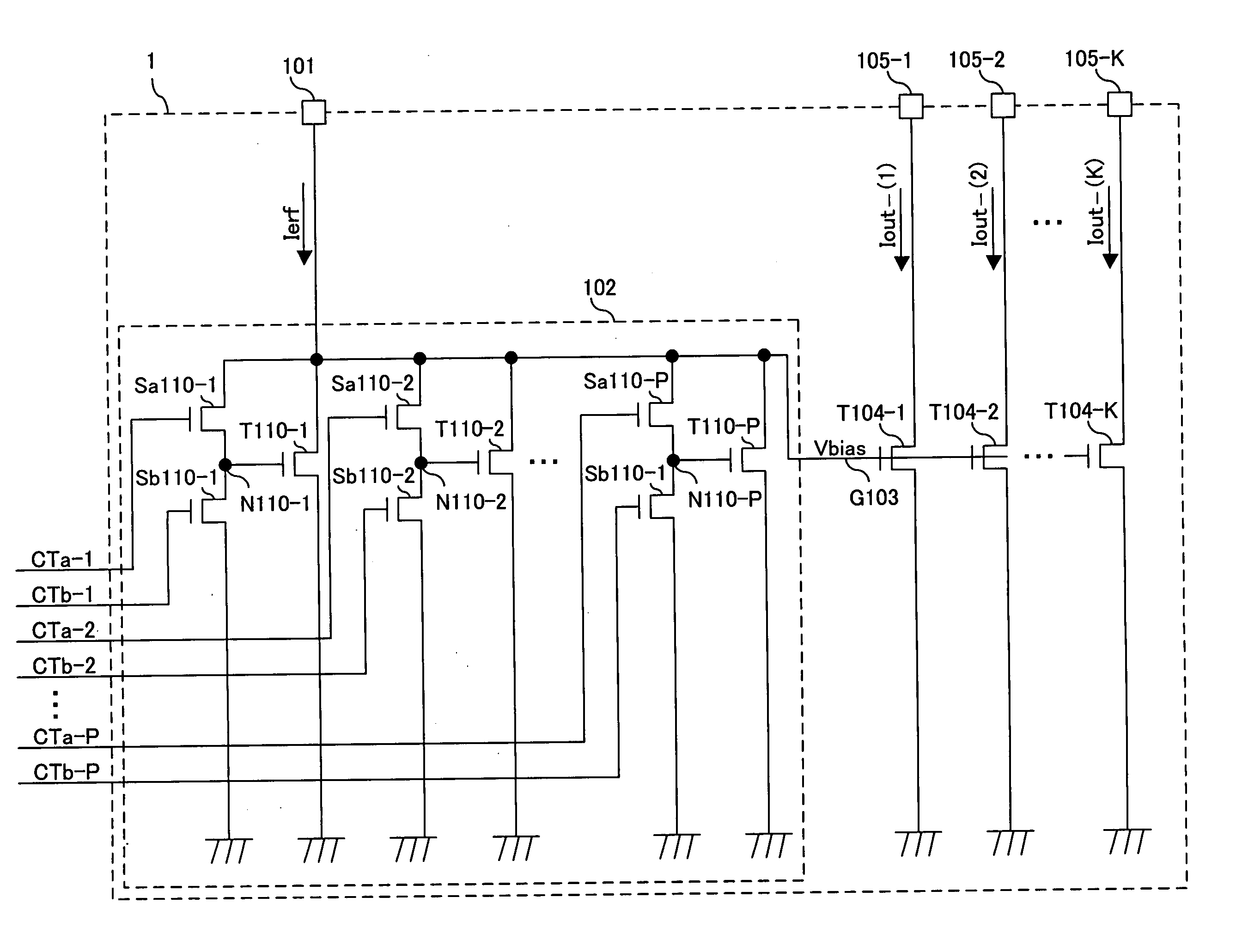
[0174] When the current driver 1 of FIG. 1 includes, instead of the bias voltage generation section 102 of FIG. 1, a bias voltage generation section 102-1 of FIG. 4, the same effects can be achieved. The bias voltage generation section 102-1 of FIG. 4 includes the voltage generation transistors T110-1 through T110-P of FIG. 1 and selection transistors Sc110-1 though Sc110-P. The voltage generation transistor T110-1 and the selection transistor Sc110-1 are connected in series between an input terminal 101 and a ground node. The selection transistor Sc110-1 is connected between the input terminal 101 and the voltage generation transistor T110-1 and receives a control signal CTc-1 from the outside at a gate thereof. The voltage generation transistor T110-1 is connected between the selection transistor Sc110-1 and the ground node and has a gate connected to a gate line G103. Each of the voltage generation transistors T110-2 through T110-P and an assoc...

second embodiment

[0177]

[0178] An overall configuration of a current driver according to a second embodiment of the present invention is shown in FIG. 5. A current driver 2 according to this embodiment includes, in addition to the components of the current driver 1 of FIG. 1, a supply power source 201, a condition storage section 202 and a control section 203.

[0179] The supply power source 201 supplies a read voltage to the condition storage section 202. The read voltage is a voltage indicating a connection state of the condition storage section 202. The control section 203 refers to the read voltage to check the connection state of the condition storage section 202.

[0180] The condition storage section 202 includes F fuses h2-1 through h2-F (where F is a natural number). Each of the fuses h2-1 through h2-F is made of a material capable of changing from a conductive state to a nonconductive state when being blown by application of a laser or a large current. With a state (i.e., blown or not blown) o...

third embodiment

[0244] Overall Configuration>

[0245] An overall configuration of a current driver 3 according to a third embodiment of the present invention is shown in FIG. 7. The current driver 3 includes, in addition to the components of the current driver 1 of FIG. 1, a storage section 301 and a control section 303. The storage section 301 is a rewritable memory such as a DRAM (dynamic random access memory) and a SRAM (static random access memory). The data signal DATA from the outside is written in the storage section 301. The control section 302 reads out the data signal DATA written in the storage section 301 and outputs the control signals CTa-1 through CTa-P and the control signals CTb-1 through CTb-P corresponding to the read-out data signal DATA to the bias voltage generation section 102.

[0246]

[0247] Next, the operation of the current driver 3 of FIG. 7 will be described. Except for the operations of the storage section 301 and the control section 302, the operation of the current driver...


PUM


Abstract

A current driver includes a gate line having a first and second nodes, K driving transistors, a terminal and a voltage generation section. The terminal receives a first current. The voltage generation section generates a bias voltage according to a current value of the first current. The gate line receives, at one of the first and second nodes, the bias voltage generated by the voltage generation section. Gates of the K transistors are connected between the first and second nodes of the gate line. In the voltage generation section, the relationship between the first current and the bias voltage is adjusted in the first mode, according to a current value of an output current flowing in a first driving transistor of the K driving transistors, and in the second mode, according to a current value of an output current flowing in a second driving transistor of the K driving transistors.

Description

CROSS-REFERENCE TO RELATED APPLICATION [0001] The disclosure of Japanese Patent Application No. 2004-373076 filed on Dec. 24, 2004 including specification, drawings and claims are incorporated herein by reference in its entirety. BACKGROUND OF THE INVENTION [0002] 1. Field of the Invention [0003] The present invention relates to a current driver and a current driving method for generating a plurality of currents. [0004] 2. Prior Art [0005] In order to drive a large-screen display panel in which display elements such as organic EL (electro luminescence) elements and the like are formed, a current driving apparatus capable of generating a plurality of driving currents is needed. Therefore, there have been cases where two separate semiconductor chips each of which includes a current driving apparatus thereon and which are placed adjacent to each other are used to form a current driving apparatus. [0006] In general, characteristics of transistors formed on the semiconductor chips vary b...

Claims


Application Information

Patent Timeline
Patent Type & Authority Applications(United States)
IPC IPC(8): H03B1/00H05B44/00
CPCG09G3/3225G09G3/3283G09G2320/0233
Inventor KOJIMA, HIROSHIOMORI, TETSUROMIZUKI, MAKOTOHIROKANE, YASUHIROKONDO, HIROSHI
Owner GK BRIDGE 1
Why Eureka
Try Eureka