
Liquid crystal display device and fabricating method thereof

Inactive Publication Date: 2006-06-29
LG DISPLAY CO LTD
View PDF3 Cites 18 Cited by
  • Summary
  • Abstract
  • Description
  • Claims
  • Application Information

AI Technical Summary

Benefits of technology

[0017] Accordingly, the present invention is directed to a liquid crystal display device that substantially obviates one or more of the problems due to limitations and disadvantages of the related art. An advantage of the present invention is to provide a thin film transistor substrate of a horizontal electric field applying type and a fabricating method thereof that simplify a process.

Problems solved by technology

Particularly, because the thin film transistor substrate includes a semiconductor process and requires a plurality of mask processes, it has a complicated fabricating process which is a major factor in the increased manufacturing costs of the liquid crystal display panel.
The thin film transistor substrate in the liquid crystal display of a horizontal electric field applying type also requires a plurality of mask processes which is a drawback of a complicated fabricating process.

Method used


Image

  • Liquid crystal display device and fabricating method thereof
  • Liquid crystal display device and fabricating method thereof
  • Liquid crystal display device and fabricating method thereof

Examples


Embodiment Construction

[0034] Reference will now be made in detail to embodiments of the present invention, examples of which are illustrated in the accompanying drawings.

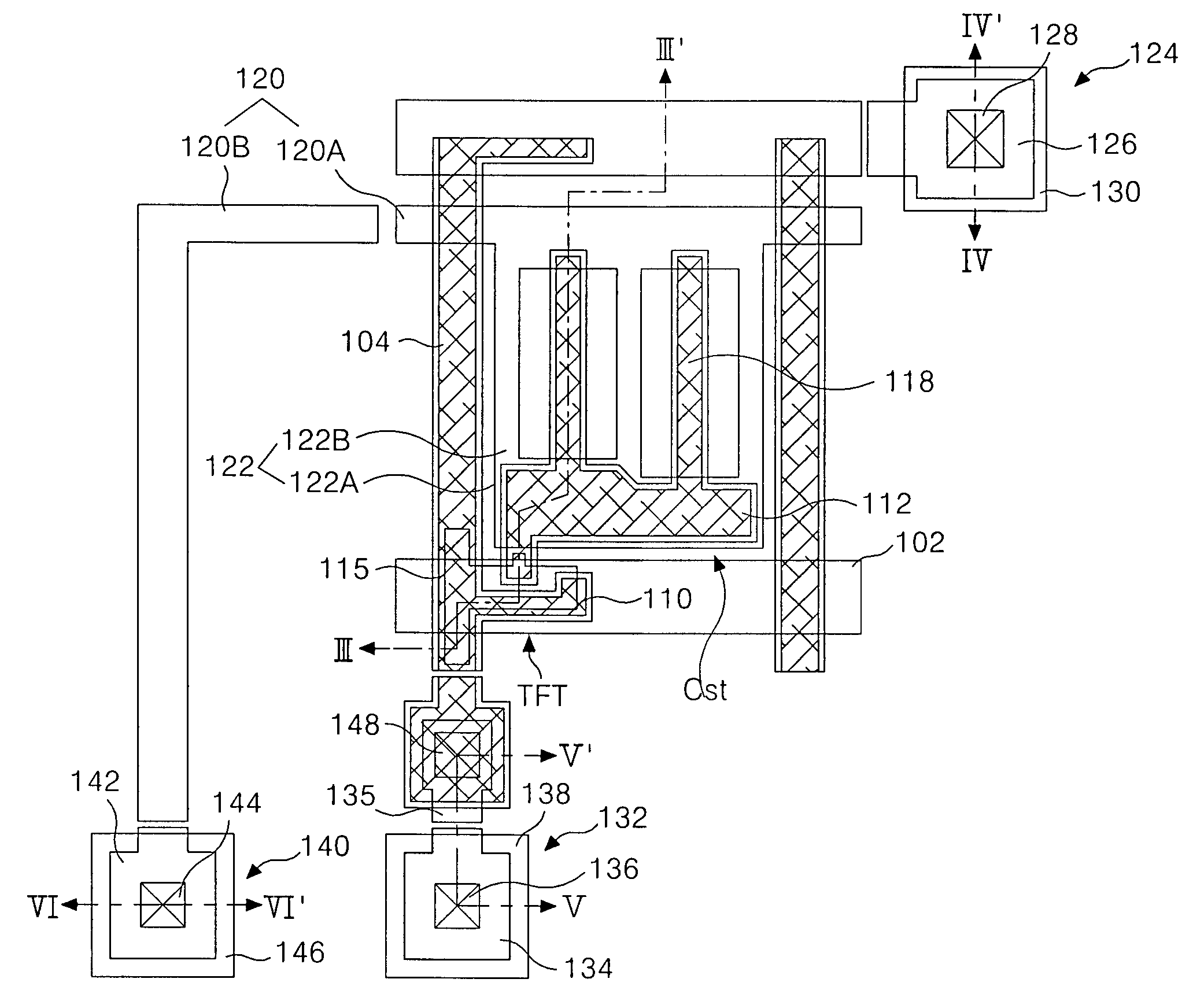
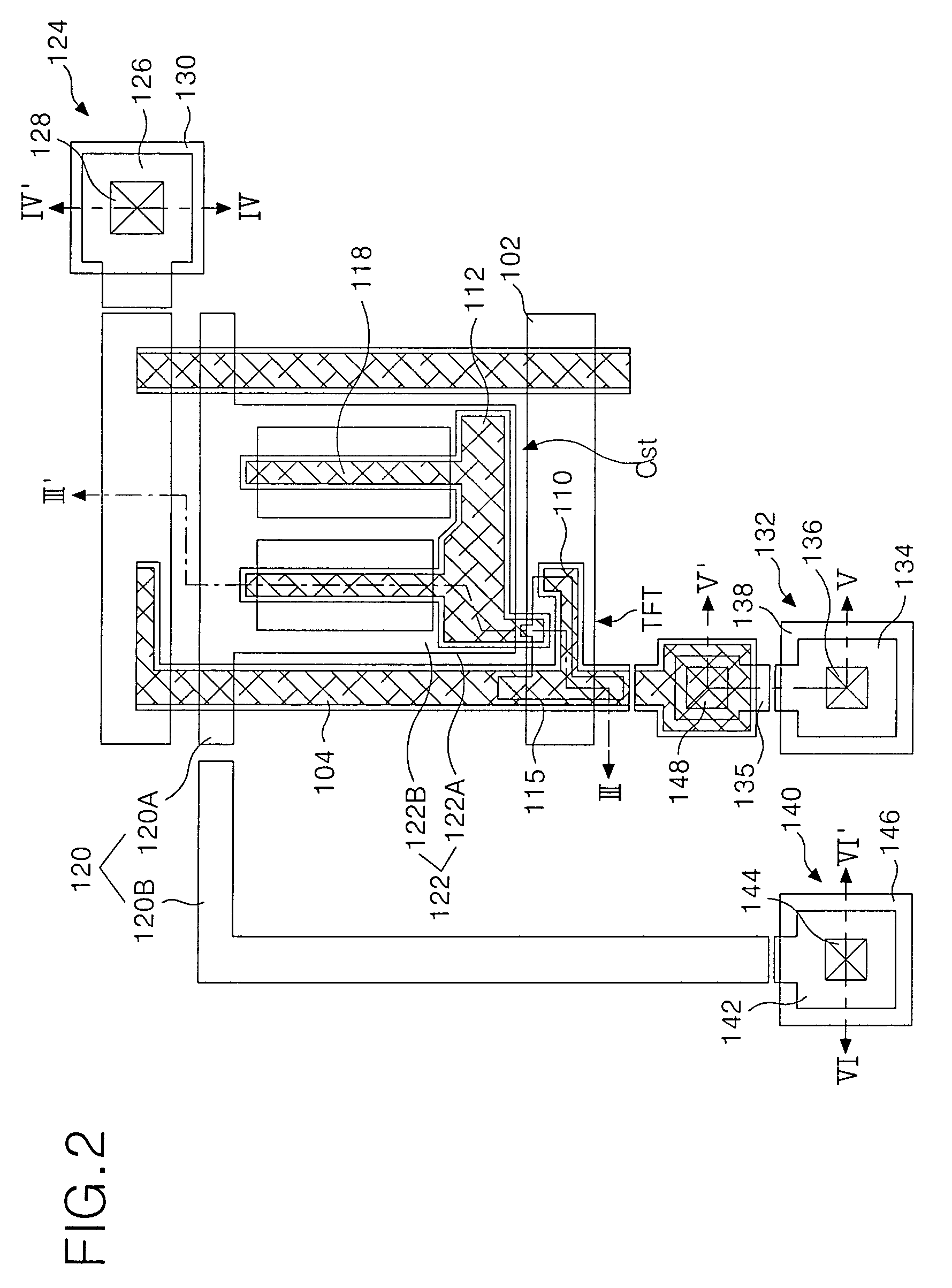
[0035]FIG. 2 is a plan view showing a structure of a thin film transistor substrate of a horizontal electric field applying type according to an embodiment of the present invention, and FIG. 3 is a section view of the thin film transistor substrate taken along III-III′, IV-IV′, V-V′ and VI-VI′ lines in FIG. 2.

[0036] Referring to FIG. 2 and FIG. 3, the thin film transistor substrate of a horizontal electric field applying type includes a gate line 102 and a data line 104 provided on a lower substrate 150 in such a manner to cross each other with a gate insulating film 152 therebetween and define a pixel area, a thin film transistor TFT connected to the gate line 102, the data line 104, a pixel electrode 118, the pixel electrode 118 and a common electrode 122 provided to form a horizontal electric field at said pixel area, a common line ...


PUM


Abstract

A liquid crystal display device and a fabricating method having a simplified process are disclosed. The liquid crystal display device compromises, among other features, first and second substrates, a gate line crossing a data line with a gate insulating film therebetween to define a pixel area. A common line is provided on the substrate substantially parallel to the gate line, and a common electrode is extended from the common line into the pixel area. A pixel electrode is extended from a drain electrode into the pixel area to form a horizontal electric field with the common electrode. The data line, a source electrode, a drain electrode and the pixel electrode are formed of a first conductive layer group having at least double conductive layers, and are formed in an area to be sealed by a sealant upon joining the first and second substrates.

Description

[0001] This application claims the benefit of Korean Patent Application No. P2004-112577 filed in Korea on Dec. 24, 2004, which is hereby incorporated by reference for all purposes as if fully set forth herein. BACKGROUND OF THE INVENTION [0002] 1. Field of the Invention [0003] This invention relates to a liquid crystal display device using a horizontal electric field, and more particularly to a thin film transistor substrate of a horizontal electric field applying type and a fabricating method thereof that simplify a process. [0004] 2. Discussion of the Related Art [0005] Generally, a liquid crystal display (LCD) controls light transmittance of a liquid crystal having a dielectric anisotropy using an electric field to display a picture. To this end, the LCD includes a liquid crystal display panel for displaying a picture by a liquid crystal cell matrix, and a driving circuit for driving the liquid crystal display panel. [0006] In FIG. 1, a related art liquid crystal display panel i...

Claims


Application Information

Patent Timeline
IPC IPC(8): G02F1/1345
CPCG02F1/134363G02F1/1362G02F2001/13629G02F1/13629G02F1/136
Inventor AHN, BYUNG CHUL
Owner LG DISPLAY CO LTD
Learn More