Multilayer chip capacitor and method for manufacturing the same

a multi-layer chip capacitor and capacitor technology, applied in the direction of fixed capacitors, stacked capacitors, fixed capacitor details, etc., can solve the problems of multi-layer chip capacitors being likely to malfunction, the reliability of multi-layer chip capacitors being affected by the negative influence of capacitors, etc., to prevent the short between the internal electrode and the external electrode, improve reliability, and prevent local thickness variation

Inactive Publication Date: 2006-06-29
SAMSUNG ELECTRO MECHANICS CO LTD
View PDF4 Cites 31 Cited by
  • Summary
  • Abstract
  • Description
  • Claims
  • Application Information

AI Technical Summary

Benefits of technology

[0022] The screen patterns may be formed such that the width of each screen pattern is greater than the distance between the screen patterns. For this purpose, the screen patterns may be arranged to partially overlap each other in the width direction. In this case, the width of each screen pattern is greater than the distance between the cutting lines arranged in the width direction. As a result, the capacitor of the invention may have the lead portion having a narrower width than that of the main electrode portion. Additionally, even if misalignment of the cutting lines occurs, undesired short between the internal electrodes and the external electrodes can be prevented.
[0023] According to the invention, the chip-protecting members are formed on both sides of the capacitor body without forming the widthwise margin portion, thereby preventing local thickness variation from being created in the multilayer chip capacitor and the electrical short on both sides of the internal electrodes. Accordingly, the cracks can be avoided on the capacitor, and reliability thereof can be enhanced.

Problems solved by technology

Such a thickness difference of the chip capacitor causes cracks of the chip capacitor, in particular, during a sintering process, and is a negative influence on reliability of the capacitor.
Accordingly, when completely manufacturing the multilayer chip capacitor by forming the external electrodes on the stack, the multilayer chip capacitor is likely to malfunction due to the cracks.
However, it is difficult to print internal electrodes having a thickness of about 1 μm with current screen printing technology.
On the other hand, although an approach has been suggested, wherein the thickness difference is complemented by printing dielectric slurries on a portion where the thickness difference occurs, this approach requires additional processes, and fails to completely solve the problem of cracks resulting from the thickness difference.
As such, due to complicated processes, this method is not only ineffective in terms of cost and time, but also difficult to secure uniformity of wet etching.

Method used


Image

  • Multilayer chip capacitor and method for manufacturing the same
  • Multilayer chip capacitor and method for manufacturing the same
  • Multilayer chip capacitor and method for manufacturing the same

Examples


Embodiment Construction

[0035] Preferred embodiments will now be described in detail with reference to the accompanying drawings. It should be noted that the embodiments of the invention can be modified in various shapes, and that the present invention is not limited to the embodiments described herein. The embodiments of the invention are described so as to enable those having an ordinary knowledge in the art to have a perfect understanding of the invention. Accordingly, shape and size of components of the invention are enlarged in the drawings for clear description of the invention. Like components are indicated by the same reference numerals throughout the drawings.

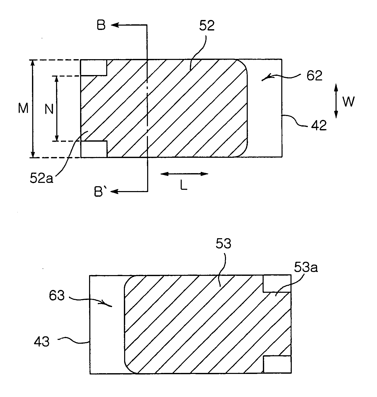
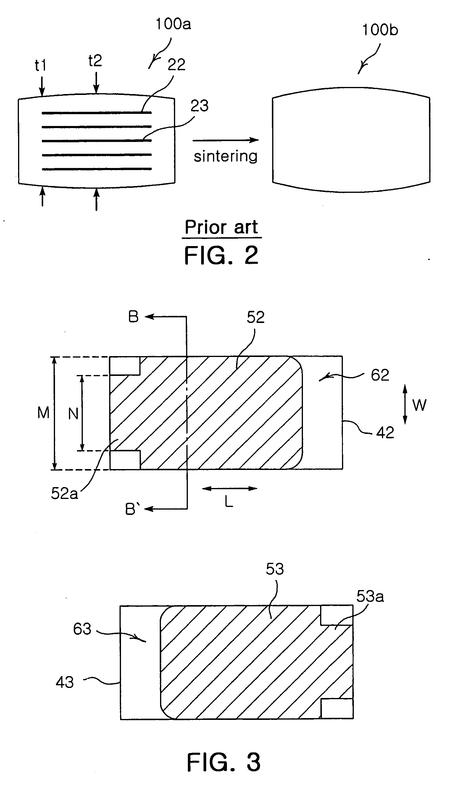
[0036]FIG. 3 is plan views illustrating a first internal electrode and a second internal electrode of a multilayer chip capacitor in accordance with one preferred embodiment of the present invention. Referring to FIG. 3, a first internal electrode 52 and a second internal electrode 53 are formed on dielectric layers 42 and 43, respectively. ...


PUM

PropertyMeasurementUnit
thicknessaaaaaaaaaa
widthaaaaaaaaaa
polarityaaaaaaaaaa

Abstract

A multilayer chip capacitor, and a method for manufacturing the same are Provided. The capacitor comprises a capacitor body having a plurality of dielectric layers stacked therein, a plurality of first and second internal electrodes formed on the dielectric layers, each of the internal electrodes including a main electrode portion and a lead portion, chip-protecting side members formed on both sides of the capacitor body to contact both sides of the first and second internal electrodes, and a pair of external electrodes formed on the outer surface of the capacitor body. The width of the main electrode portion is the same as that of the dielectric layers, and the width of the lead portion is smaller than that of the dielectric layers.

Description

RELATED APPLICATION [0001] The present invention is based on, and claims priority from, Korean Application Number 2004-110924, filed Dec. 23, 2004, the disclosure of which is incorporated by reference herein in its entirety. BACKGROUND OF THE INVENTION [0002] 1. Field of the Invention [0003] The present invention relates to a multilayer chip capacitor, and, more particularly, to a multilayer chip capacitor, designed to avoid occurrence of cracks caused by a thickness difference and short circuit caused by misalignment of cutting lines, thereby enhancing reliability of devices, and a method for manufacturing the same. [0004] 2. Description of the Related Art [0005] Generally, a multilayer chip capacitor (MLCC) comprises a plurality of dielectric layers referred to as ceramic green sheets and internal electrodes formed between the plurality of dielectric layers. Since such a multilayer chip capacitor can realize a higher electrostatic capacitance with a small size while being easily m...

Claims


Application Information

Patent Timeline
Patent Type & Authority Applications(United States)
IPC IPC(8): H01G4/228
CPCH01G4/012H01G4/232Y10T29/435Y10T29/413Y10T29/417H01G4/30
Inventor KIM, HYOUNG HOSHIN, HYO SOONCHOO, HO SUNG
Owner SAMSUNG ELECTRO MECHANICS CO LTD
Why Eureka
Try Eureka