
Eureka
For R&D, Eureka makes reading and utilizing patents & technical documents easy.
Eureka AIR
Designed for self-driven R&D workflows. Generate viable solutions, solve complex R&D challenges, empower your innovation with AI.

Eureka Materials
Designed for material experts only. Revolutionize your material R&D, from search, analyze, to developing new materials.

TechResearch
Generate reliable direction feasibility study reports for your R&D in just a few steps.

TechSeek
Discover and master advanced knowledge NOW. Basics, ideas, possibilities, all at once.

TechMind
As an expert in R&D Theories, TechMind can generates customized viable solutions instantly.

TechRisk
Analyze your overall solution with one click, know your potential R&D risks in advance.

TechMonitor
Get weekly tech updates, stay abreast of the latest tech innovations and key insights.
Semiconductor device
- Summary
- Abstract
- Description
- Claims
- Application Information
AI Technical Summary
Benefits of technology
Problems solved by technology
Method used
Image

Examples
second embodiment
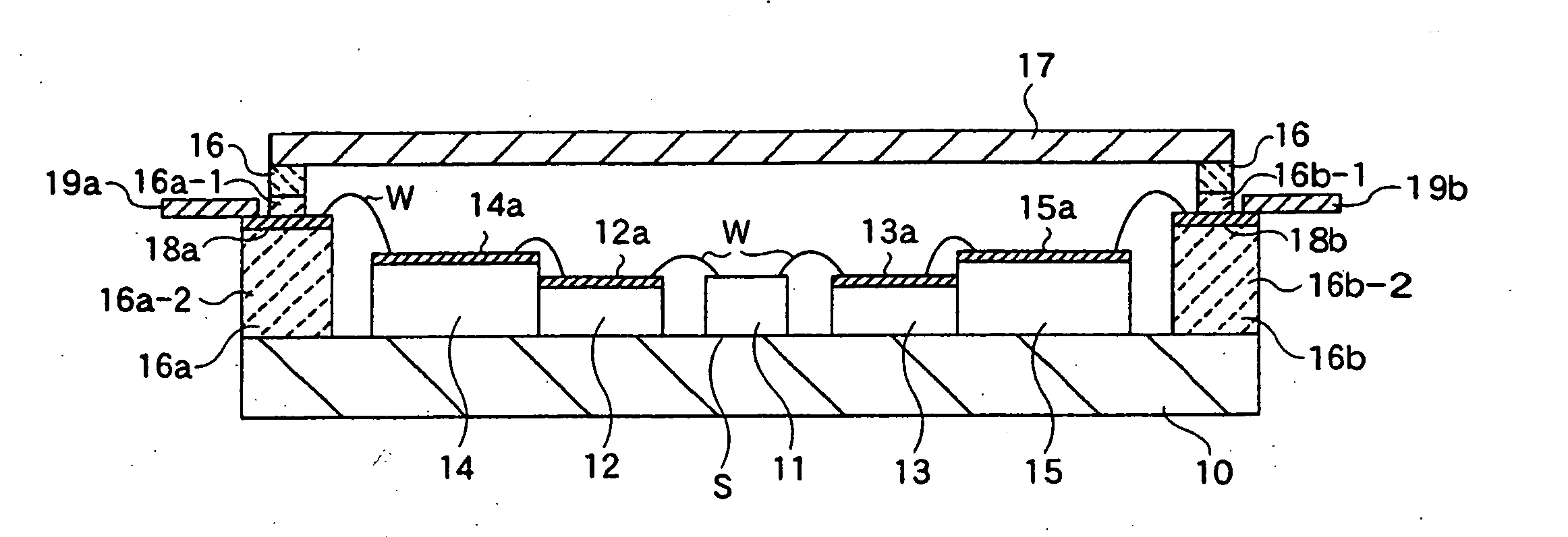
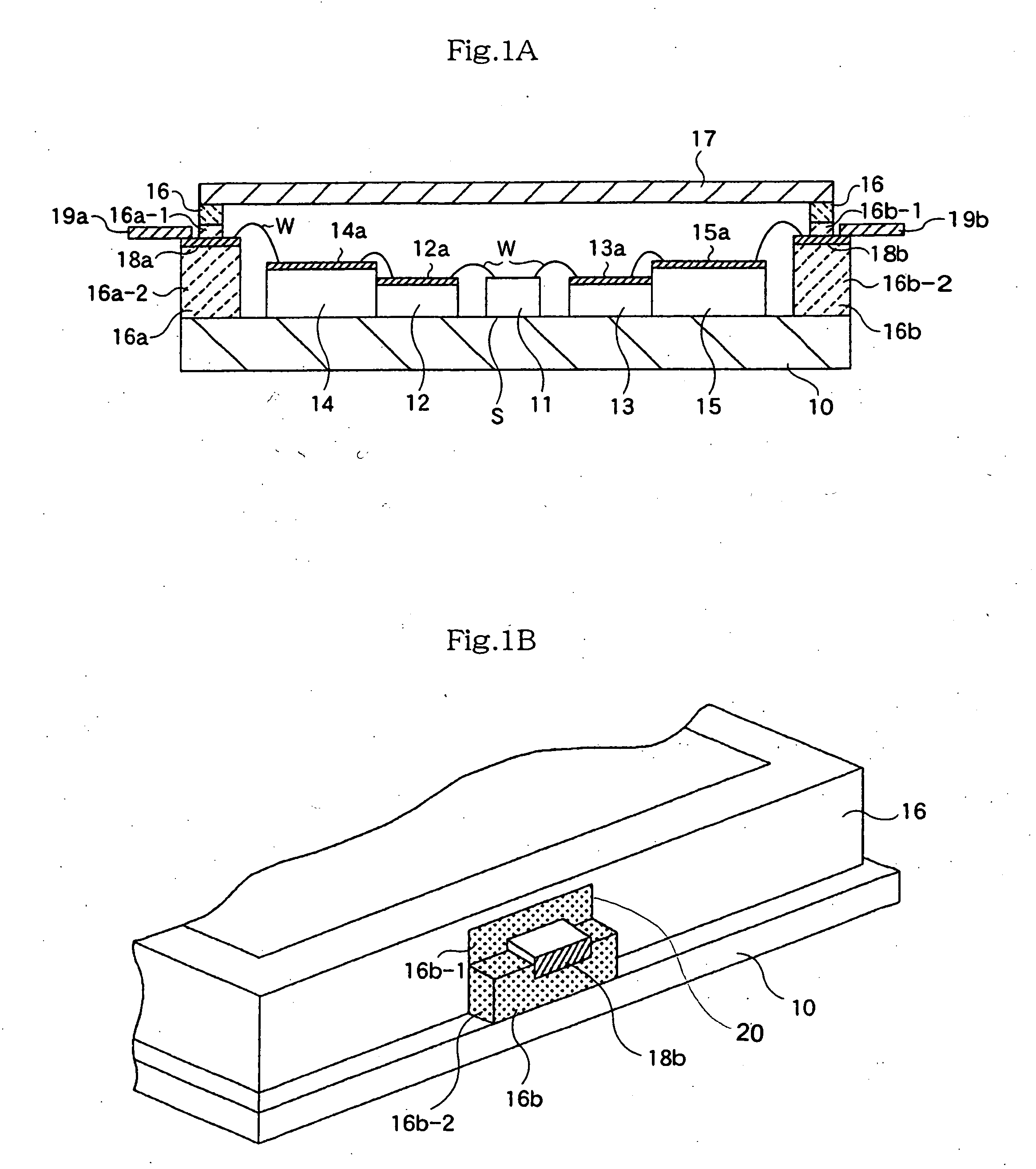
[0033] Next, a semiconductor device according to the present invention is explained referring to FIG. 2. The semiconductor device of the embodiment has a structure in which the input and output side are substantially symmetrical with a semiconductor element (not illustrated) similar to the semiconductor device shown in FIG. 1. FIG. 2 is a cross section showing only the output side portion of the semiconductor device. In this figure, parts corresponding to the parts of the semiconductor device shown in FIG. 1 are assigned with the same symbols and some duplicated explanations are omitted.
[0034] In the embodiment, a fifth dielectric plate 21 with a line conductor 21a on its surface is arranged between the fourth dielectric plate 15 and the band-shaped conductor 18b. The fifth dielectric plate 21 has a thickness the surface of which is positioned at substantially the same height as the band-shaped conductor 18b with respect to the main surface S of the base plate 10.
[0035] In the neig...
third embodiment
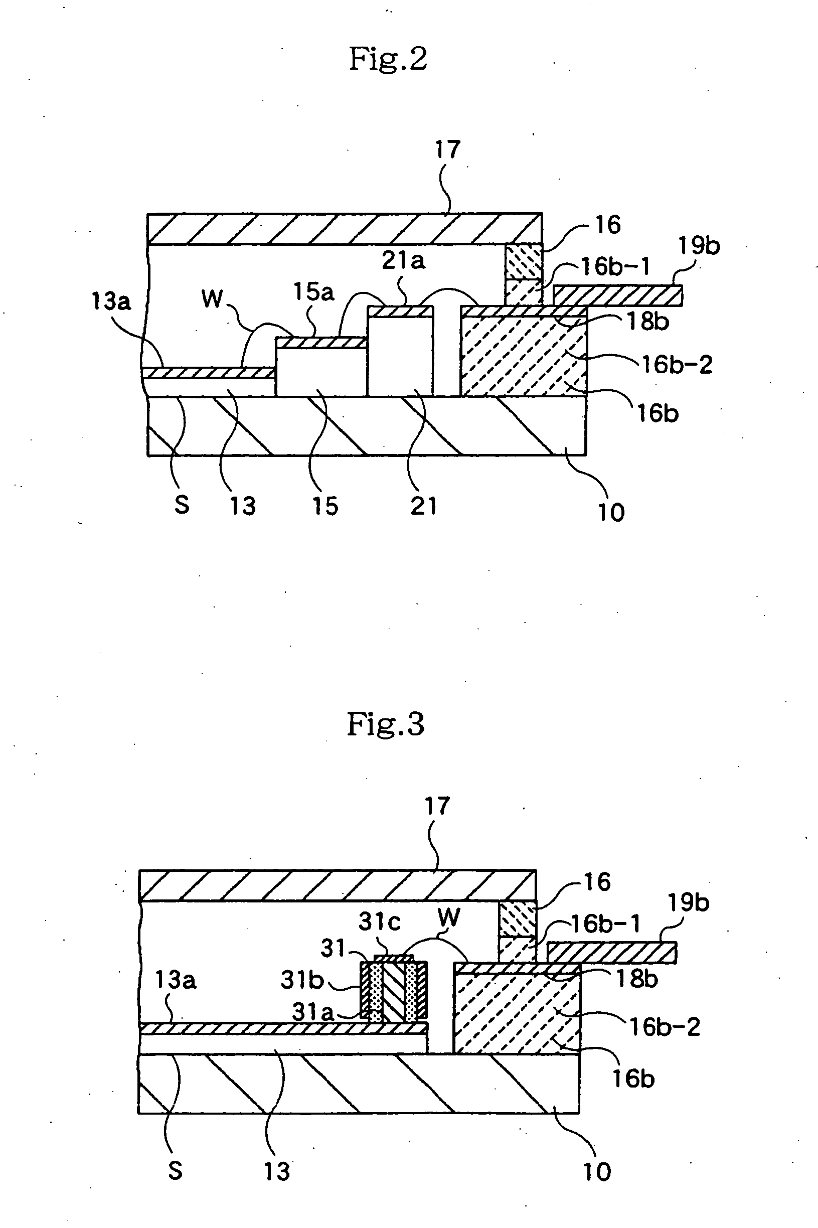
[0037] A semiconductor device according to the present invention is explained referring to FIG. 3. The semiconductor device of the embodiment has a substantially symmetric structure of the input and output side with respect to the semiconductor element (not illustrated), which is similar to the semiconductor device shown in FIG. 1 or in FIG. 2. FIG. 3 is a cross sectional view showing only the output side portion of the semiconductor device. In this figure, parts corresponding to those of the semiconductor device shown in FIG. 1 are assigned with the same symbols and duplicated explanations are omitted.
[0038] In this embodiment, an insulator block 31 is arranged on the end portion adjacent to the band-shaped conductor 18b on the second dielectric plate 13. On the insulator block 31, a VIA hole 31a, which is a through hole, is formed and a conduction layer 31b is formed on side surfaces surrounding the VIA hole 31a. On the insulator block 31, a conducting pattern 31c, which is connec...
fourth embodiment
[0042] the present invention will be explained referring to FIG. 4. The semiconductor device of the embodiment has a substantially symmetric structure of the input and output side with respect to the semiconductor element (not illustrated), which is similar to the semiconductor device shown in FIG. 1. FIG. 4 is a cross section showing only the output portion of the semiconductor device. In this figure, parts corresponding to the parts of the semiconductor device shown in FIG. 1 are assigned with the same symbols and duplicated explanations are omitted.
[0043] In this embodiment, a stepped surface 41 lower than the main surface S is provided on a part of the base plate 10. A sidewall 16 is formed on the stepped surface 41 to make the height of the circuit pattern 13a equal to the height of the band-shaped conductor 18b.
[0044] Also with the structure, forming the sidewall 16 on the step surface 41 can decrease the difference in the height of the circuits to be connected with each othe...
PUM
 Abstract
Description
Claims
Application Information
 - R&D Engineer
- R&D Manager
- IP Professional
- Industry Leading Data Capabilities
- Powerful AI technology
- Patent DNA Extraction
Browse by: Latest US Patents, China's latest patents, Technical Efficacy Thesaurus, Application Domain, Technology Topic, Popular Technical Reports.
© 2024 PatSnap. All rights reserved.Legal|Privacy policy|Modern Slavery Act Transparency Statement|Sitemap|About US| Contact US: help@patsnap.com