Double-layer conductive thin film-based transparent broadband electromagnetic wave absorber

A technology of conductive film and wave absorber, which is applied in the direction of electrical components, antennas, etc., can solve the problem of narrow application range of wave absorber, and achieve the effect of ensuring broadband wave absorption effect, expanding application range, and high mechanical hardness

Active Publication Date: 2016-10-26
XIDIAN UNIV
View PDF5 Cites 37 Cited by
  • Summary
  • Abstract
  • Description
  • Claims
  • Application Information

AI Technical Summary

Problems solved by technology

[0005] The purpose of the present invention is to overcome the above-mentioned defects in the prior art, and propose a transparent broadband electromagnetic absorber based on a double-layer conductive film. By using transparent materials, high light transmittance is achieved, which is used to solve the problem of existing absorbers. Technical issues with narrow application

Method used


Image

  • Double-layer conductive thin film-based transparent broadband electromagnetic wave absorber
  • Double-layer conductive thin film-based transparent broadband electromagnetic wave absorber
  • Double-layer conductive thin film-based transparent broadband electromagnetic wave absorber

Examples


Embodiment 1

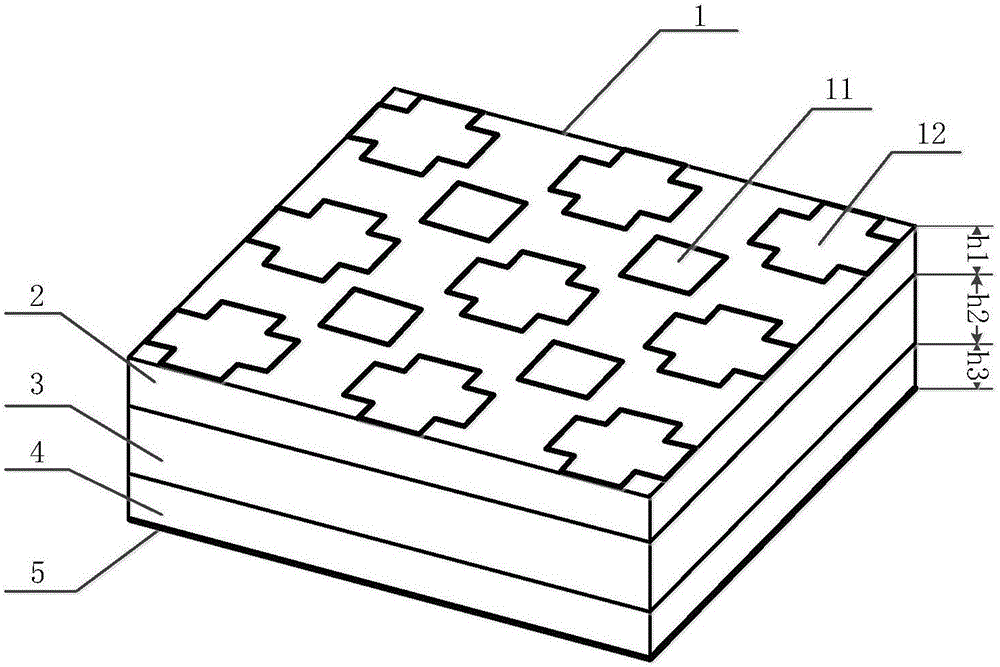
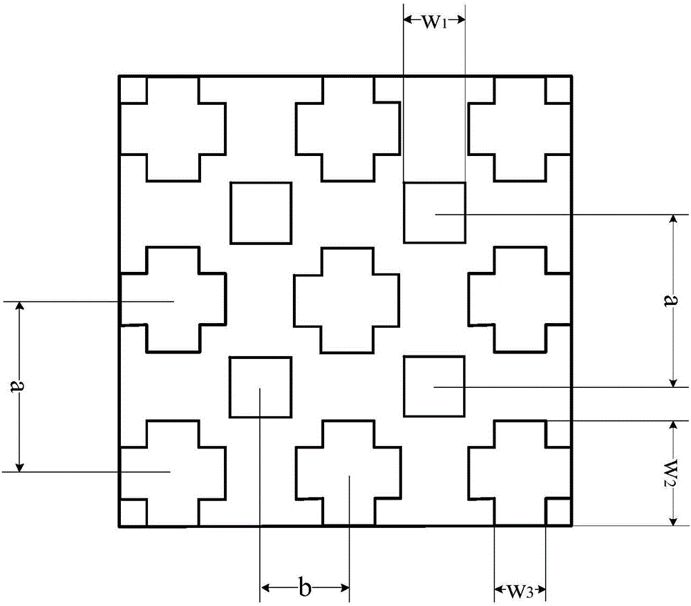
[0024] refer to figure 1 , including a conductive film 1, a first dielectric layer 2, a second dielectric layer 3, a third dielectric layer 4 and a bottom plate 5, wherein the three dielectric layers 2, 3 and 4 are arranged from top to bottom to form a stacked dielectric layer The bottom plate 5 is printed on the lower surface of the third dielectric layer 4, and the conductive film 1 is printed on the upper surface of the first dielectric layer 2, and the conductive film 1 is an array composed of m×n square transparent conductive films 11 and (m +1)×(n+1) arrays composed of cross-shaped transparent conductive films 12 are composited. In this embodiment, an array composed of 2×2 square transparent conductive films 11 and 3×3 cross-shaped transparent conductive films are used An array composed of 12, its specific structure is as follows figure 2 shown.

[0025] Both the first dielectric layer 2 and the third dielectric layer 4 adopt a relative permittivity ε r1 2.7 square p...

Embodiment 2

[0031] Embodiment 2 has the same structure as Embodiment 1, and the following parameters have been adjusted:

[0032] Both the first dielectric layer 2 and the third dielectric layer 4 adopt a relative permittivity ε r1 A square polymethacrylate (PMMA) dielectric plate of 4, wherein the thickness h of the first dielectric layer 2 1 =1mm, the thickness h of the third dielectric layer 4 3 =1mm; the thickness h of the second dielectric layer 3 is selected 2 2mm, relative permittivity ε r2 3.9 square quartz glass dielectric plate; square conductive film 11 and cross-shaped conductive film 12 adopt square resistance R S1 The graphene film is 100Ω / sq, and the bottom layer 5 adopts square resistance R S It is a square indium tin oxide film of 10Ω / sq, and the side length of the square conductive film 11 is W 1 is 9mm.

Embodiment 3

[0034] The structure of embodiment 3 is identical with the structure of embodiment 1, and following parameter has been adjusted:

[0035] Both the first dielectric layer 2 and the third dielectric layer 4 adopt a relative permittivity ε r1 is a square polymethacrylate (PMMA) dielectric plate of 2, wherein the thickness h of the first dielectric layer 2 1 =2.5mm, the thickness h of the third dielectric layer 4 3 =2.5mm; the thickness h of the second dielectric layer 3 is selected 2 2.5mm, relative permittivity ε r2 2.7 square polycarbonate dielectric plate; square conductive film 11 and cross-shaped conductive film 12 adopt square resistance R S1 It is a graphene film of 60Ω / sq, and the bottom plate 5 adopts square resistance R S A square indium tin oxide film of 5Ω / sq.


PUM


Abstract

The invention provides a double-layer conductive thin film-based transparent broadband electromagnetic wave absorber and aims at solving the technical problem of a narrow application range of an existing wave absorber. The double-layer conductive thin film-based transparent broadband electromagnetic wave absorber comprises a conductive thin film, a first dielectric layer, a second dielectric layer, a third dielectric layer and a bottom plate, wherein transparent dielectric plates are adopted as the first dielectric layer and the third dielectric layer; the transparent dielectric plate or an air dielectric is adopted as the second dielectric layer; the three dielectric layers are arranged from top to bottom to form the dielectric layers with a stacked structure; a transparent conductive thin film is adopted as the bottom plate and is printed on the lower surface of the third dielectric layer; and the conductive film is formed by compounding m*n arrays formed by square transparent conductive thin films and (m+1)*(n+1) arrays formed by cross-shaped transparent conductive thin films and is printed on the upper surface of the first dielectric layer. High light transmission is achieved while the wave absorption bandwidth and the wave absorption rate are ensured; and the double-layer conductive thin film-based transparent broadband electromagnetic wave absorber can be applied to electromagnetic anti-interference of microwave systems, of aircraft cabin glass, a PCB-based novel inter-chip wireless interconnection system and the like, requiring the high light transmission.

Description

technical field [0001] The invention belongs to the field of microwave electromagnetic stealth technology, and relates to a transparent broadband electromagnetic absorber, in particular to a transparent broadband electromagnetic absorber based on a double-layer conductive film, which can be used for electromagnetic anti-interference in fields requiring high light transmission and electromagnetic compatibility. Background technique [0002] With the development of electronic information technology, the impact of electromagnetic radiation on the environment is increasing day by day. At airports, aircraft flights are sometimes delayed due to electromagnetic interference; in hospitals, mobile phones often interfere with the normal work of various electronic medical instruments. Therefore, controlling electromagnetic pollution and finding a wave-absorbing device that can resist and weaken electromagnetic radiation has become a major topic in electromagnetics. On the other hand, ...

Claims


Application Information

Patent Timeline
Patent Type & Authority Applications(China)
IPC IPC(8): H01Q17/00
CPCH01Q17/00
Inventor 吴边薛宝玥赵雨桐张兴飞
Owner XIDIAN UNIV
Why Eureka
Try Eureka