

Copper electrodeposition in microelectronics
a technology of copper electrodes and microelectronics, applied in the field of microelectronics manufacture, can solve the problems of interconnection size, metal filling challenges, and disturbing electrical characteristics of the connected device, and achieve the effect of rapid bottom-up deposition
- Summary
- Abstract
- Description
- Claims
- Application Information
AI Technical Summary
Benefits of technology
Problems solved by technology
Method used
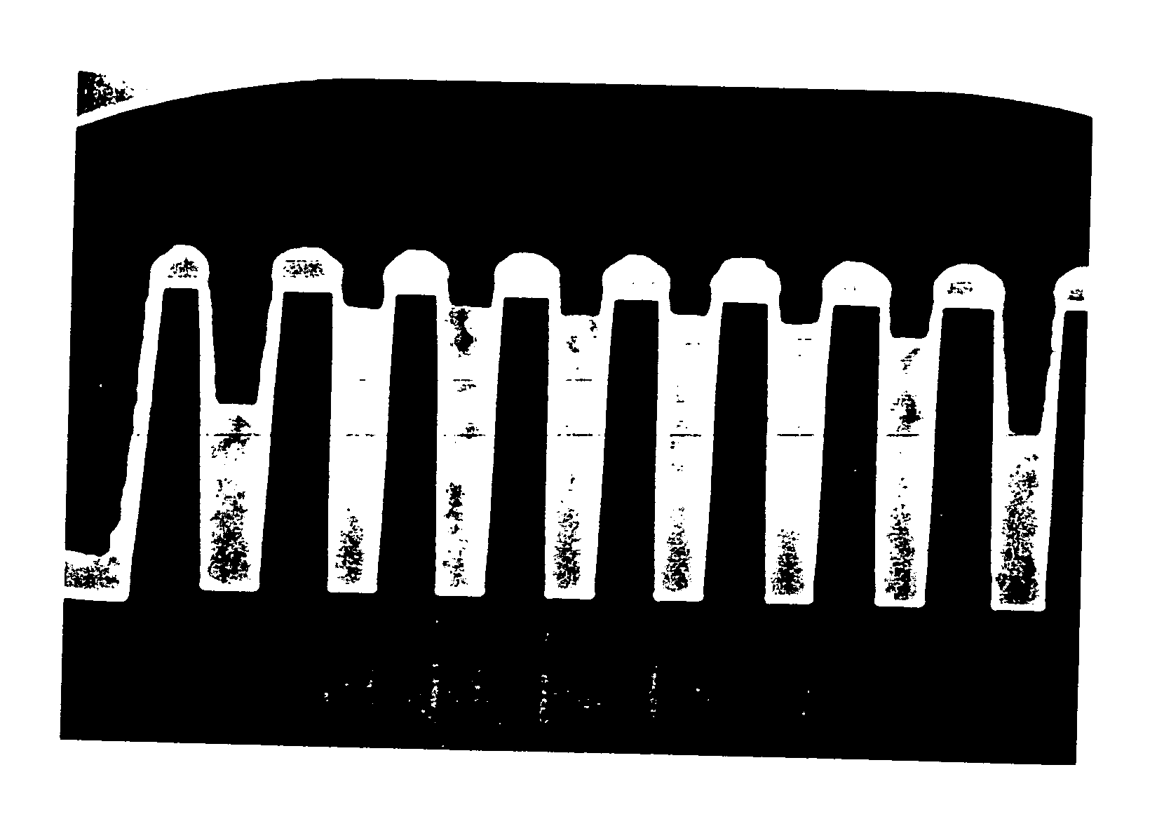
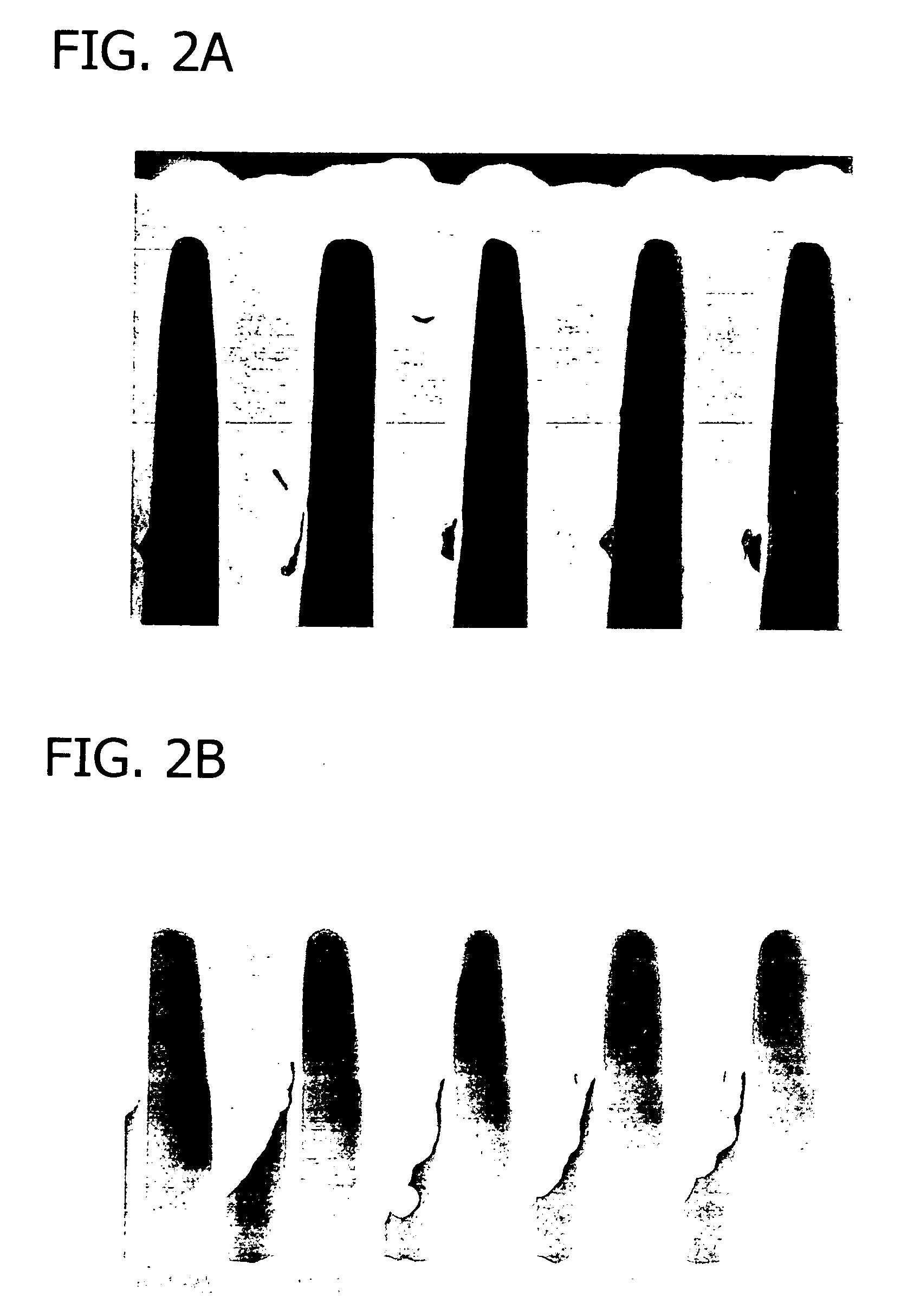
Image

Examples
example 1
Low Acid / High Cu Superfill Electrolytic Plating Bath with Suppressor of the Invention
[0067] To superfill a small diameter / high aspect ratio integrated circuit device feature, a Low acid / High Cu electrolytic plating bath was prepared comprising the following components: [0068] 160 g / L CuSO4.5H2O (copper sulfate pentahydrate) [0069] 10 g / L H2SO4 (concentrated sulfuric acid) [0070] 50 mg / L Chloride ion [0071] 9 mL / L ViaForm® Accelerator [0072] 200 mg / L of Cationic Suppressor (PO / EO block copolymer of ethylenediamine having a MW of 5500 g / mol corresponding to structure (5)).
[0073] The bath (1 L) was prepared as follows. CUSO4.5H2O (160 g) was fully dissolved in deionized water. Concentrated sulfuric acid (10 g) was added followed by addition of hydrochloric acid sufficient to yield 50 mg chloride ion in solution. Deionized water was added for a total volume of 1 liter. The final plating bath was prepared by further addition of ViaForm Accelerator (9 mL) and PO / EO block copolymer of et...
example 2
High Acid / Low Cu Superfill Electrolytic Plating Bath with Suppressor of the Invention
[0080] To superfill a small diameter / high aspect ratio integrated circuit device feature, a High Acid / Low Cu electrolytic plating bath was prepared comprising the following components: [0081] 70 g / L CuSO4.5H2O (copper sulfate pentahydrate) [0082] 180 g / L H2SO4 (concentrated sulfuric acid) [0083] 50 mg / L Chloride ion [0084] 3 mL / L ViaForm® Accelerator [0085] 400 mg / L Cationic Suppressor (PO / EO block copolymer of ethylenediamine having a MW of 5500 g / mol corresponding to structure (5)).
example 3
Mid acid / High Cu Superfill Electrolytic Plating Bath with Suppressor of the Invention
[0086] To superfill a small diameter / low aspect ratio integrated circuit device feature, a Mid acid / High Cu electrolytic plating bath was prepared comprising the following components: [0087] 200g / L CUSO4.5H2O (copper sulfate pentahydrate) [0088] 80 g / L H2SO4 (concentrated sulfuric acid) [0089] 50 mg / L Chloride ion [0090] 8 mL / L ViaForm® Accelerator [0091] 200 mg / L Cationic Suppressor (PO / EO block copolymer of ethylenediamine having a MW of 5500 g / mol corresponding to structure (5)) [0092] 4 mL / L ViaForm® L700.
PUM
| Property | Measurement | Unit |
|---|---|---|
| concentration | aaaaa | aaaaa |
| concentration | aaaaa | aaaaa |
| depth:width | aaaaa | aaaaa |
Abstract
Description
Claims
Application Information