
Apparatus and process for treating dielectric materials

a dielectric material and apparatus technology, applied in the direction of heating, cleaning using liquids, therapy, etc., can solve the problems of insufficientness for the smaller devices of the future, inability to integrate and in general difficulty in integrating porous low-k materials in the manufacture of semiconductor devices

Inactive Publication Date: 2006-06-29
AXCELIS TECHNOLOGIES
View PDF10 Cites 86 Cited by
  • Summary
  • Abstract
  • Description
  • Claims
  • Application Information

AI Technical Summary

Benefits of technology

[0007] Disclosed herein Disclosed herein are apparatuses and processes for treating dielectric materials such as low k dielectrics, premetal dielectrics, and the like for advanced semiconductor devices. In one embodiment, the apparatus comprises a radiation source module comprising a reflector, an ultraviolet radiation source, and a plate transmissive to the wavelengths of about 150 nm to about 300 nm, to define a sealed interior region, wherein the sealed interior region is in fluid communication with a first fluid source; a process cham...

Problems solved by technology

Considerable attention has been focused on electrically isolating the conductors from each other using new insulators having low dielectric constants because although silica (SiO2), which has traditionally been used in such devices because of its relatively low dielectric constant of about 4, met the requirements of earlier (i.e., larger) applications, it will not be adequate for the smaller devices of the future.
However, the integration of porous low-k materials in the manufacture of the semiconductor device, in general, has proven difficult.
No ultraviolet radiation apparatus currently exists that addresses the special problems and concerns associated with curing and / or removing porogens from various dielectric materials.

Method used


Image

  • Apparatus and process for treating dielectric materials
  • Apparatus and process for treating dielectric materials
  • Apparatus and process for treating dielectric materials

Examples


examples

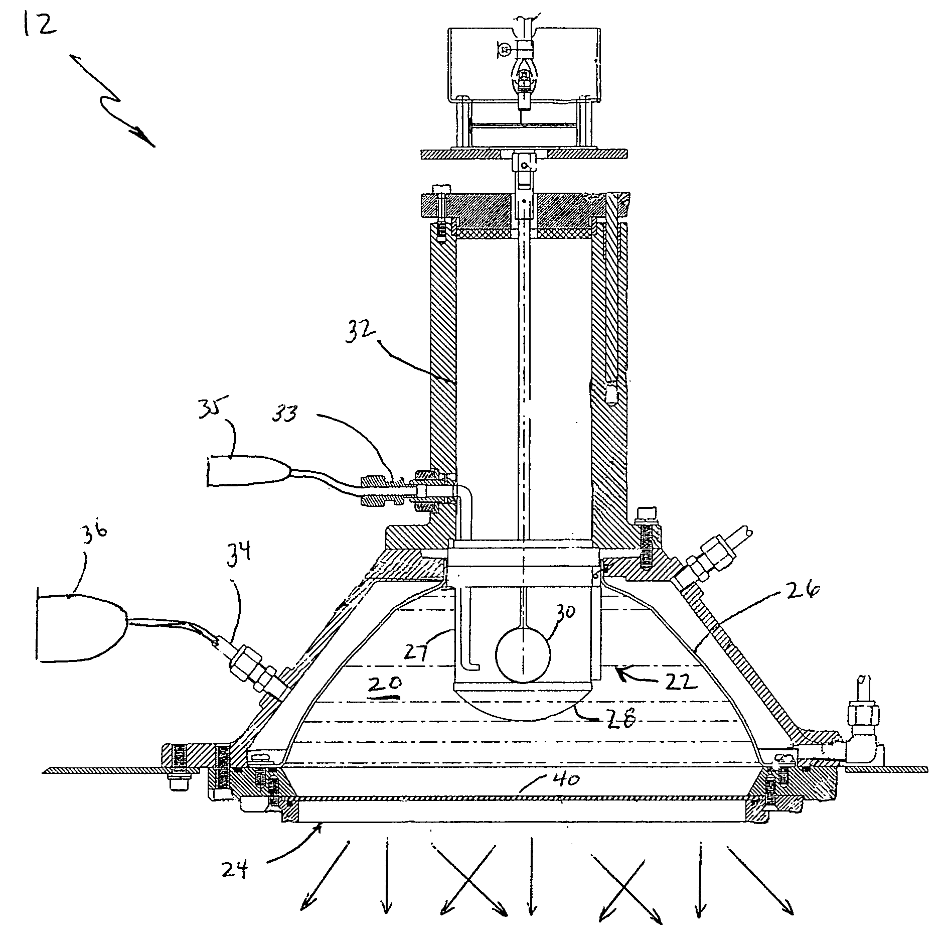
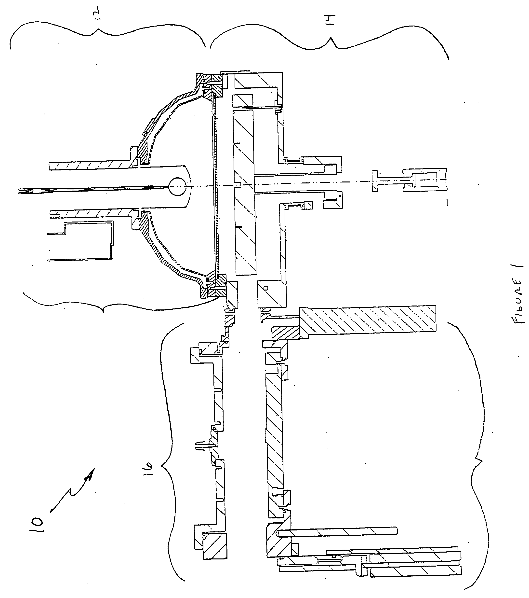
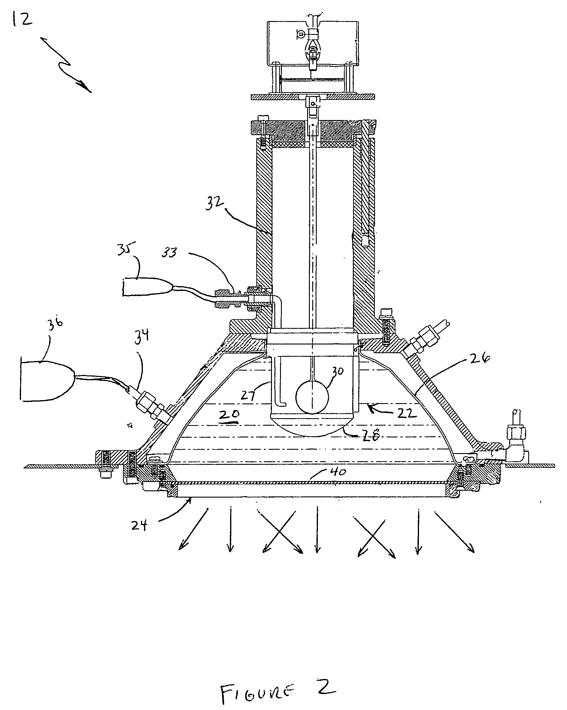
[0062] In this example, multiple substrates including the same dielectric material were processed in the Apparatus as described above. FIG. 12 graphically illustrates the effectiveness of the periodic in situ clean function. The in situ clean process included flowing an oxidizing fluid into the process chamber and exposing the oxidizing fluid to the ultraviolet broadband radiation. The irradiance probe measured intensity of the ultraviolet broadband radiation into the process chamber. As a result of outgassing and contaminant deposition onto the transmissive plate during processing of multiple substrates containing the dielectric material, transmission of the ultraviolet broadband radiation decreases as a function of processed substrates. Periodically cleaning the process chamber cleans the plate so as to substantially restore transmission of the ultraviolet broadband radiation. Advantageously, the walls and other surfaces of the process chamber can also be presumed to have been cle...


PUM

PropertyMeasurementUnit
Temperatureaaaaaaaaaa
Fractionaaaaaaaaaa

Abstract

Apparatuses and processes for treating dielectric materials such as low k dielectric materials, premetal dielectric materials, barrier layers, and the like, generally comprise a radiation source module, a process chamber module coupled to the radiation source module; and a loadlock chamber module in operative communication with the process chamber and a wafer handler. The atmosphere of each one of the modules can be controlled as may be desired for different types of dielectric materials. The radiation source module includes a reflector, an ultraviolet radiation source, and a plate transmissive to the wavelengths of about 150 nm to about 300 nm, to define a sealed interior region, wherein the sealed interior region is in fluid communication with a fluid source.

Description

CROSS REFERENCE TO RELATED APPLICATIONS [0001] The present application relates to and claims priority to U.S. Provisional Application No. 60 / 581,185 filed on Jun. 18, 2004, incorporated herein by reference in its entirety.BACKGROUND [0002] This disclosure generally relates to an apparatus for curing and / or removing porogens from dielectric materials, and in particular, to an apparatus for curing and / or removing porogens from low k dielectric materials with ultraviolet radiation in a controlled environment. [0003] As semiconductor and other microelectronic devices progressively decrease in size, the demands placed on device components continue to increase. For example, the prevention of capacitive crosstalk between interconnect lines becomes significantly more important with smaller devices. Capacitive crosstalk is generally a function of both the distance between conductors and the dielectric constant (k) of the material placed in between the conductors. Considerable attention has b...

Claims


Application Information

Patent Timeline
IPC IPC(8): C23C16/00H01L21/31H01L21/26
CPCH01L21/312H01L21/324Y10S134/902H01L21/02348H01L21/02334
Inventor WALDFRIED, CARLOGARMER, CHRISTOPHERESCORCIA, ORLANDOBERRY, IVAN IIISAKTHIVEL, PALANIJANOS, ALAN C.
Owner AXCELIS TECHNOLOGIES
Features
  • Generate Ideas
  • Intellectual Property
  • Life Sciences
  • Materials
  • Tech Scout
  • Unparalleled Data Quality
  • Higher Quality Content
  • 60% Fewer Hallucinations
Learn More