Direct memory access circuit and disk array device using same

a memory access circuit and disk array technology, applied in the direction of electric digital data processing, instruments, computing, etc., can solve the problems of insufficient protection of descriptors and data cannot be guaranteed, and achieve the effect of preventing data corruption due to address failure and highly reliable system

Active Publication Date: 2006-06-29
FUJITSU LTD
View PDF7 Cites 1 Cited by
  • Summary
  • Abstract
  • Description
  • Claims
  • Application Information

AI Technical Summary

Benefits of technology

[0036] In this way, for both the reading and writing of descriptors, data corruption due to an address failure can be prevented. In particular, an address failure of memory where address lines and data l

Problems solved by technology

In this way, data is protected by the above mentioned check code and the ECC in the data transfer operation by the DMA engine 102, but protection of the descriptors is not sufficient.
In particular, the address during DMA transfer is not protected, so if a failure is generated in the add

Method used


Image

  • Direct memory access circuit and disk array device using same
  • Direct memory access circuit and disk array device using same
  • Direct memory access circuit and disk array device using same

Examples


first embodiment

of the Disk Array Device

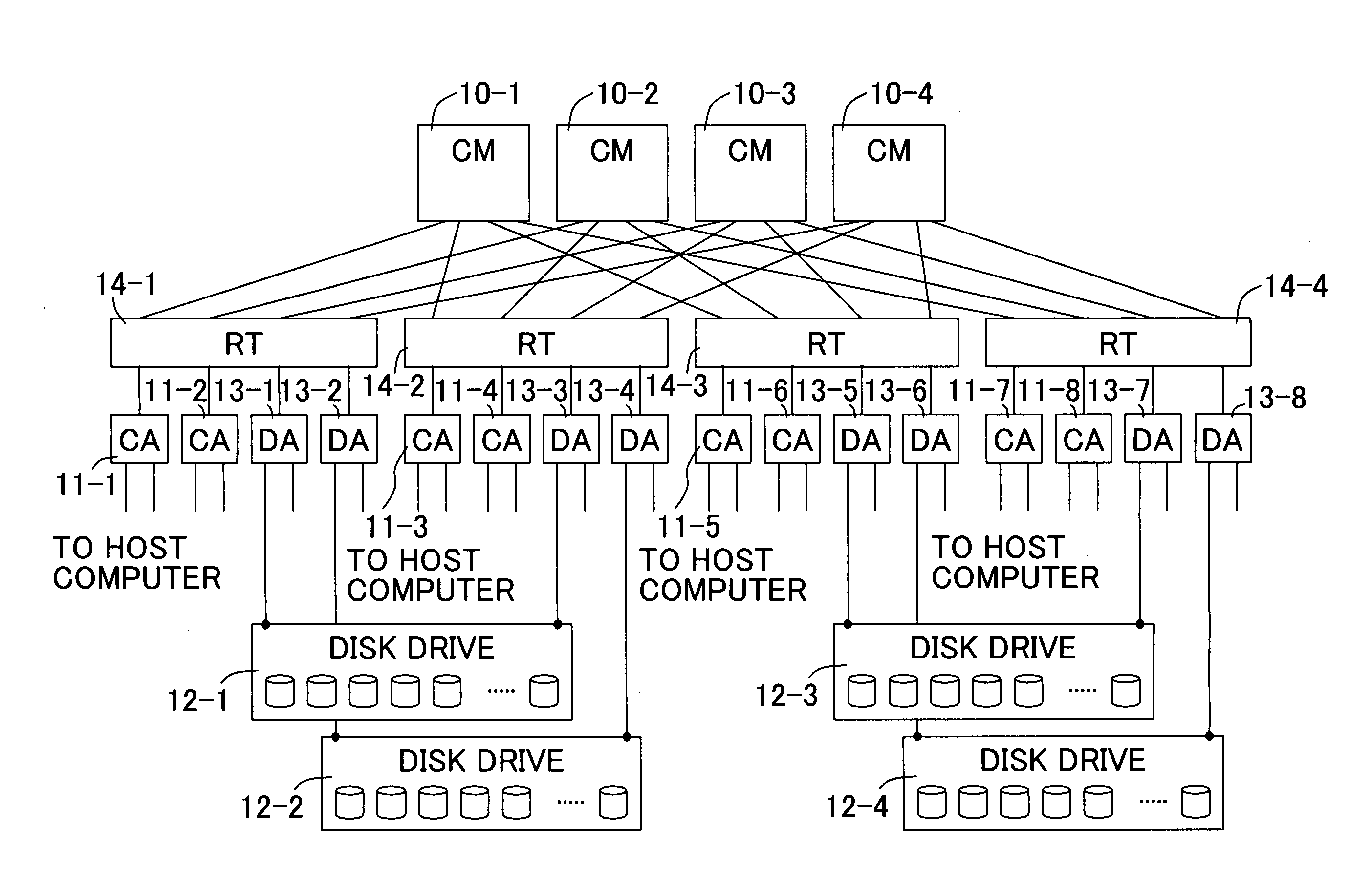
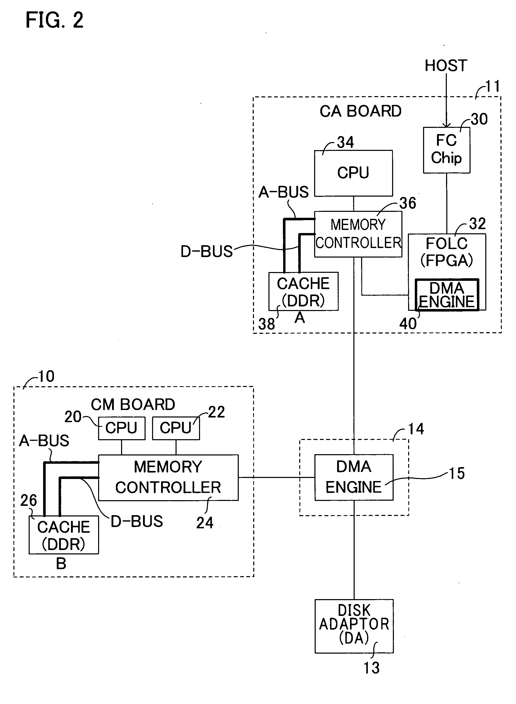
[0048]FIG. 1 is a block diagram depicting a general configuration of the first embodiment of the disk array apparatus of the present invention and FIG. 2 is a block diagram depicting details of the major section in FIG. 1.

[0049] As FIG. 1 shows, the disk array apparatus includes cache managers (“CM” in FIG. 1) 10-1 to 10-4, which are major units having a cache memory and cache control unit respectively, channel adapters (CA in FIG. 1) 11-1 to 11-8, which are interfaces with the host computer (not illustrated), disk devices 12-1 to 12-4 having a plurality of disk drives, and device adapters (DA in FIG. 1) 13-1 to 13-8, which are interfaces with these disk devices 12-1 to 12-4.

[0050] The disk array apparatus further includes routers (RT in FIG. 1) 14-1 to 14-4, which interconnect the cache managers 10-1 to 10-4, channel adapters 11-1 to 11-8 and device adapters 13-1 to 13-8 for performing data transfer and communication among these major units.

[0051] This di...

second embodiment

of Disk Array Apparatus

[0109]FIG. 7 is a block diagram depicting the second embodiment of the disk array apparatus according to the present invention, and FIG. 8 is a block diagram depicting details of the major section thereof. As FIG. 7 shows, the disk array apparatus is connected to two host computers 17-1 and 17-2 by the fiber channel links 18-1 and 18-2.

[0110] The disk array apparatus is comprised of the host adapters 11-1 and 11-2 which are in charge of the host interface, cache memories 26-1 and 26-2, cache controllers 10-1 and 10-2 for managing the cache memories 26-1 and 26-2, and disk adapters 13-1 and 13-2 which are in charge of the disk interfaces.

[0111] The host adapters 11-1 and 11-2, cache memories 26-1 and 26-2, cache controllers 10-1 and 10-2 and disk adapters 13-1 and 13-2 are the same as the channel adapters, cache managers and device adapters in FIG. 1 respectively.

[0112] The disk array apparatus is further comprised of the switches 16-1 and 16-2 which provide...


PUM


Abstract

A DMA circuit prevents an erroneous data transfer by a descriptor due to an address failure of memory. When a descriptor is created, the data processing unit writes a pointer, for storing the descriptor, in a predetermined part of the descriptor, and stores the descriptor in memory, and when a DMA engine reads the descriptor from the memory, the DMA engine confirms whether the value is correct, and judges whether a DMA transfer of the data in the memory is possible. For both reading and writing of a descriptor, data corruption due to an address failure can be prevented.

Description

CROSS-REFERENCE TO RELATED APPLICATIONS [0001] This application is based upon and claims the benefit of priority from the prior Japanese Patent Application No. 2004-372441, filed on Dec. 24, 2004, the entire contents of which are incorporated herein by reference. BACKGROUND OF THE INVENTION [0002] 1. Field of the Invention [0003] The present invention relates to a DMA (Direct Memory Access) circuit which directly accesses memory according to an external instruction and transfers data, and a disk array device using this, and more particularly to a DMA circuit which is suitable for guaranteeing the validity of the data on a disk array device to be used as an external storage device of a computer, and a disk array device using this. [0004] 2. Description of the Related Art [0005] As various data are computerized and handled by computers, efficiently transferring a large volume of data independently from the computer is now demanded. For this, a technology to independently access the me...

Claims


Application Information

Patent Timeline
IPC IPC(8): G06F13/28
CPCG06F3/0619G06F3/0659G06F3/0689G06F13/28G06F12/16
Inventor TAKAHASHI, HIDENORIOGAWA, YUICHIHANEDA, TERUMASA
Owner FUJITSU LTD
Why Eureka
Try Eureka