Nonvolatile memory and memory card

a technology of nonvolatile memory and memory card, applied in the field of nonvolatile memory, can solve the problem of requiring a relatively long processing time, and achieve the effect of enhancing the performance of sequential erase access

Inactive Publication Date: 2006-06-29
RENESAS TECH CORP
View PDF23 Cites 7 Cited by
  • Summary
  • Abstract
  • Description
  • Claims
  • Application Information

AI Technical Summary

Benefits of technology

[0005] An object of the present invention is to provide a nonvolatile memory capable of making data access of a relatively large size efficient.
[0040] Owing to the issue of one access command with the erase instruction command as the head by the memory controller, the nonvolatile memory is capable of making parallel the operation of erasing at one memory bank and the operation of erasing at a plurality of memory banks upon sequential access to a plurality of read processing regions. Consequently, sequential erase performance is enhanced.

Problems solved by technology

A relatively long processing time is required to obtain a desired threshold voltage at each memory cell transistor.

Method used


Image

  • Nonvolatile memory and memory card
  • Nonvolatile memory and memory card
  • Nonvolatile memory and memory card

Examples


Embodiment Construction

>

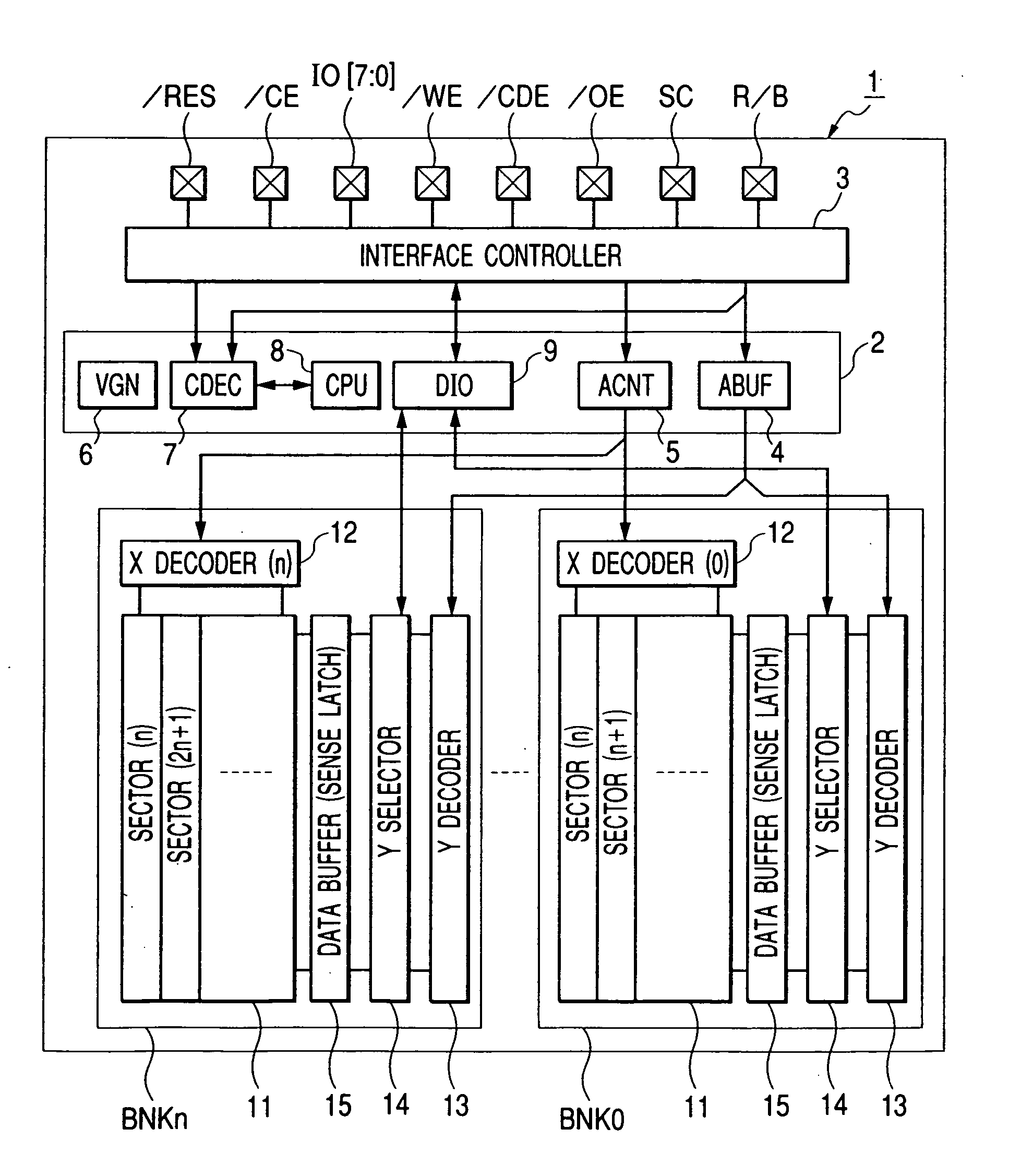
[0063] One embodiment of a flash memory 1 according to the present invention is shown overall in FIG. 1.

[0064] The flash memory 1 includes a plural, e.g., n+1 memory banks BNK0 through BNKn capable of performing memory operations independently respectively, a control unit 2 for controlling the memory operations with respect to the memory banks BNK0 through BNKn, and an interface controller 3 which interfaces with the outside, which are provided on one semiconductor substrate (semiconductor chip) like monocrystalline silicon. The control unit 2 has an address buffer (ABUF) 4, an address counter (ACNT) 5, an internal power supply circuit (VGN) 6, a command decoder (CDEC) 7, a central processing unit and its operating program (CPU) 8, and a data input / output control logic circuit (DIO) 9. The following description will be made under n=3 and the provision of four memories for convenience.

[0065] An input / output terminal I / O [7:0] used as a group, of the flash memory 1 is shared for an...


PUM


Abstract

The present invention provides a nonvolatile memory having a plurality of memory banks having a plurality of erasable and programmable nonvolatile memory cells and capable of memory operation independently respectively. The nonvolatile memory is capable of sequentially receiving write data and a write start command by the number of write processing regions after a write instruction command, a write start address and the number of the write processing regions with the write start address as a start point are inputted, latching write data for one write processing region in one memory bank and thereafter starting writing to each memory cell in response to the write start command, and making parallel a latch operation at one memory bank and writing to each memory cell at other memory banks.

Description

BACKGROUND OF THE INVENTION [0001] This invention relates to a nonvolatile memory having a plurality of memory banks and a memory card equipped with the nonvolatile memory, and to a technology effective for application to a flash memory, for example. [0002] A flash memory makes a difference in threshold voltage of each memory cell transistor according to the injection of electrons into a floating gate thereof or pulling-out thereof, for example, to thereby make it possible to store information therein. In the present specification, a state in which the threshold voltage of the memory cell transistor is low, is called an “erase state”, and a state in which the threshold voltage thereof is high, is called a “write state”, respectively. When information is stored according to write data, a high voltage is applied to a memory cell transistor held in the erase state in accordance with a logical value of write data. When the information is erased, a high voltage is applied thereto in a di...

Claims


Application Information

Patent Timeline
Patent Type & Authority Applications(United States)
IPC IPC(8): G06F12/00G06F12/06G06K19/07G11C16/02G11C16/10G11C16/16G11C16/26
CPCG11C16/10G11C16/102G11C16/16G11C16/26
Inventor MATSUSHITA, TORUNODA, SATOSHI
Owner RENESAS TECH CORP
Why Eureka
Try Eureka