Dual-mode decoder circuit, integrated circuit memory array incorporating same, and related methods of operation

a decoder circuit and integrated circuit technology, applied in digital storage, semiconductor/solid-state device details, instruments, etc., can solve the problems of extremely small pitch of difficult to interconnect word lines and bit lines within very dense arrays, and run from one end of an integrated circuit, etc., to achieve short time and short time

Active Publication Date: 2006-07-06
SANDISK TECH LLC
View PDF43 Cites 71 Cited by
  • Summary
  • Abstract
  • Description
  • Claims
  • Application Information

AI Technical Summary

Benefits of technology

[0013] During an exemplary test mode, the first of the two global word line decoders is switched to the reverse decoding mode while the second of the two global word line decoders remains in the forward decoding mode. The second global word line decoder selects and drives one global word line. The first global word line decoder, which is now a reverse decoder, detects whether there is a “hit” between the selected global word line and the input address, and drives the hit output signal accordingly. In some cases, the decoder may be configured to assert the hit signal whenever the selected global word line matches the address. In other cases, even when the selected global word line matches the address, the decoder may be configured to assert the hit signal only if the global word lines adjacent to the selected global word line are both deselected. For example, if there is a short between the selected global word line and one or both adjacent “unselected” global word lines, the dual-mode decoder may nonetheless detect a “miss” rather than a “hit.” The addresses provided to the global word line decoder may be sequenced through all possible values in a relatively short amount of time.
[0014] Continuing with the exemplary test mode, the first global word line decoder may be switched to the forward decoding mode while the second global word line decoder is switched to the reverse decoding mode. The first global word line decoder now selects and drives one global word line, while the second global word line decoder detects whether there is a “hit” between the selected global word line and the input address, and drives the hit output signal accordingly. The addresses provided to the global word line decoder may again be sequenced through all possible values in a relatively short amount of time. If the hit signal is asserted for all addresses, during both passes through the sequenced addresses, both global word line decoders may be then known to be fully functional. Moreover, if the two global word line decoders drive each global word line at the opposite ends of such global word lines, it is then known that none of the global word lines have an open somewhere along its length between the two decoders. In addition, if the dual mode decoders are configured to reject a “hit” when an adjacent global word line is also selected (or even partially selected), then it may be also known that no such shorts exist between any of the global word lines.

Problems solved by technology

Moreover, recent developments in certain memory cell technologies have resulted in word lines and bit line having an extremely small pitch.
Interfacing the word line decoders and bit line decoders to tightly spaced word lines and bit lines within very dense arrays has become extremely challenging, particularly if such array lines exist on more than one layer, as in a three-dimensional memory array having more than one plane of memory cells.
Such long lines running from one end of an integrated circuit (i.e., a “chip”) to the other end may be very resistive as well as capacitively heavily-loaded.
As a result, the propagation delay for selecting and de-selecting a long, resistive, and heavily-loaded global array line may be significant.
Such a defect could affect many local word lines in each on many array blocks.
Other potential defects in global word lines and local word lines, such as a shorted line, may require using a marching pattern to detect the failure, even with the use of dedicated test columns.
Such a test sequence requires a long test time and is therefore expensive to implement.

Method used


Image

  • Dual-mode decoder circuit, integrated circuit memory array incorporating same, and related methods of operation
  • Dual-mode decoder circuit, integrated circuit memory array incorporating same, and related methods of operation
  • Dual-mode decoder circuit, integrated circuit memory array incorporating same, and related methods of operation

Examples


Embodiment Construction

)

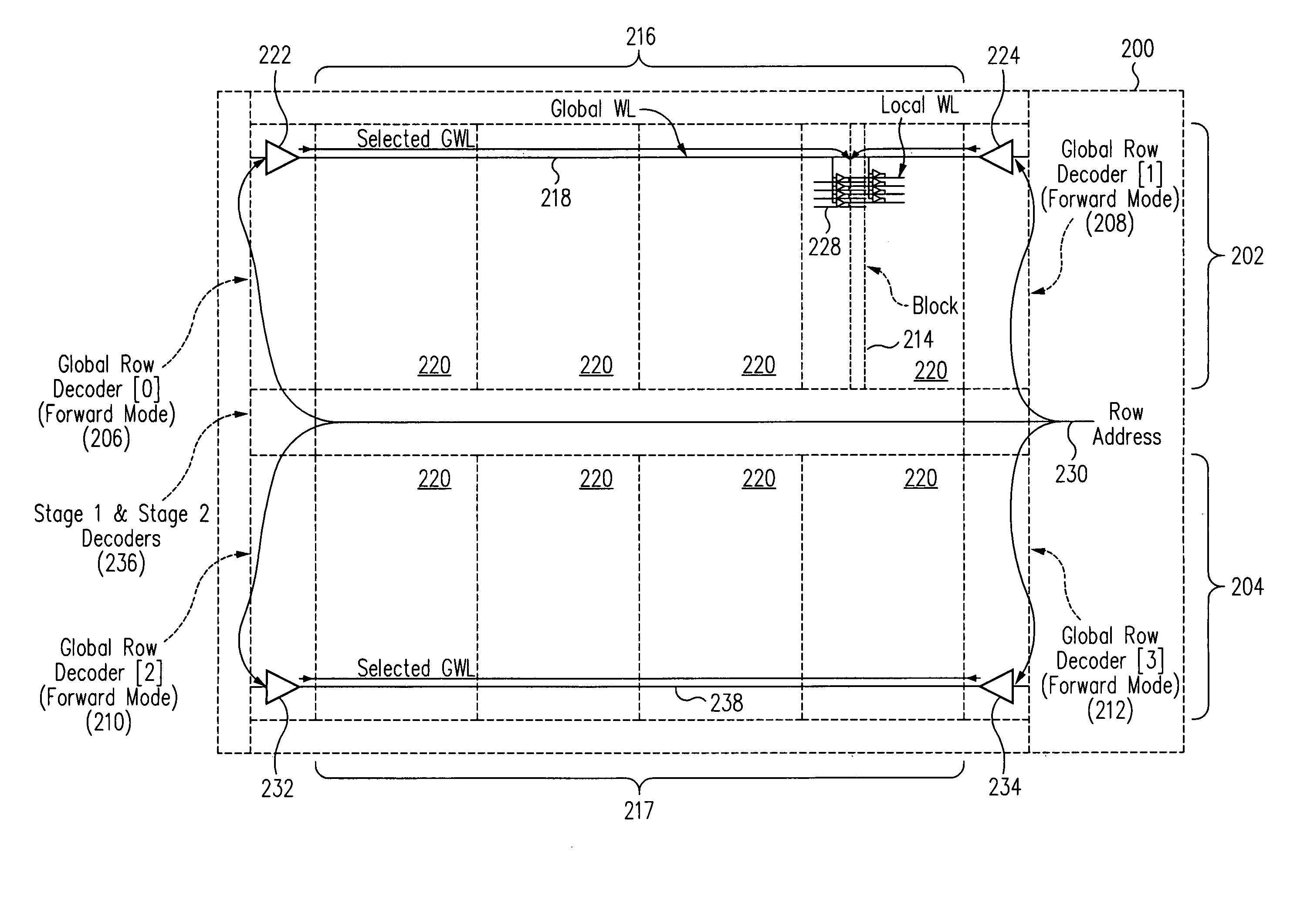
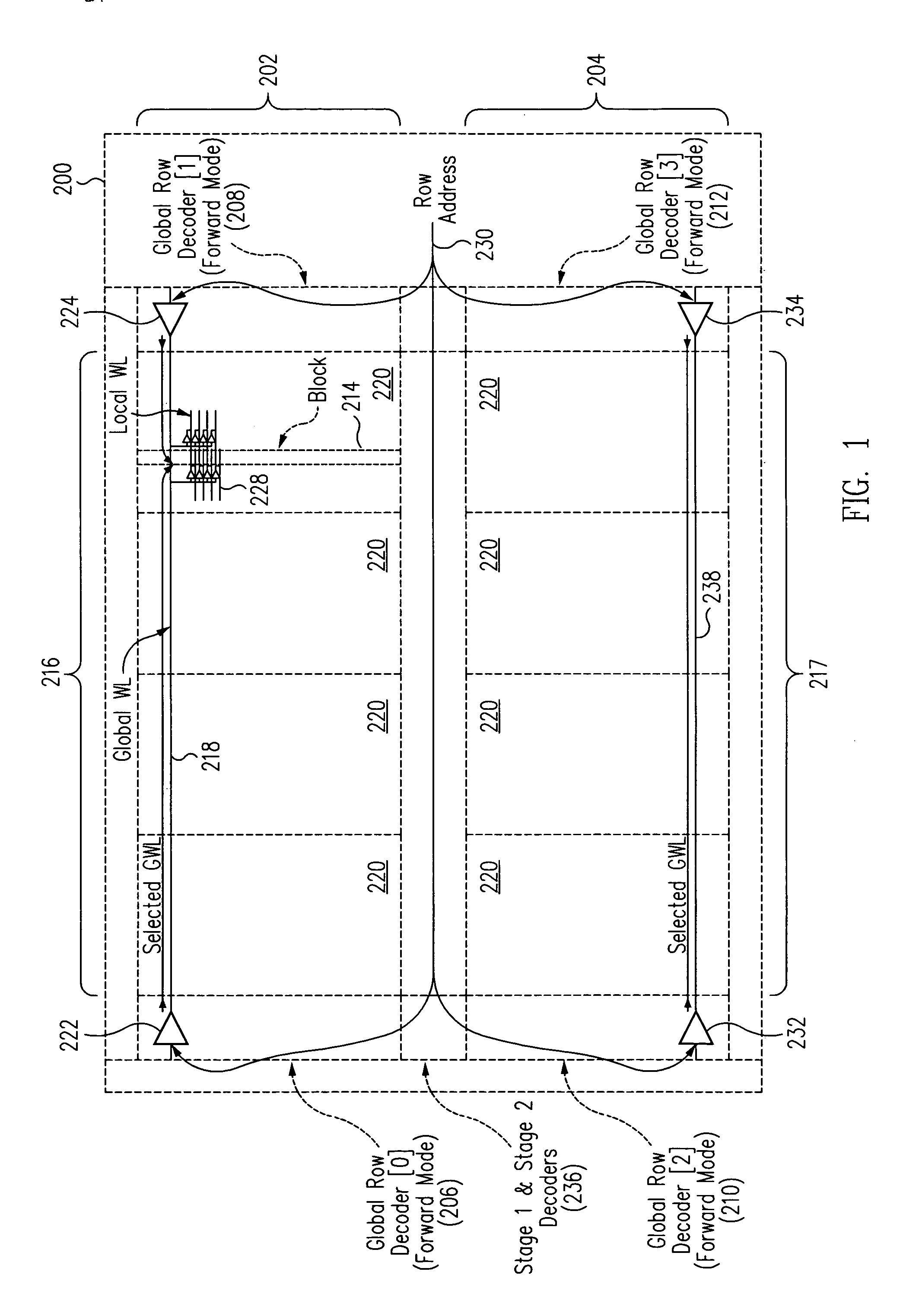
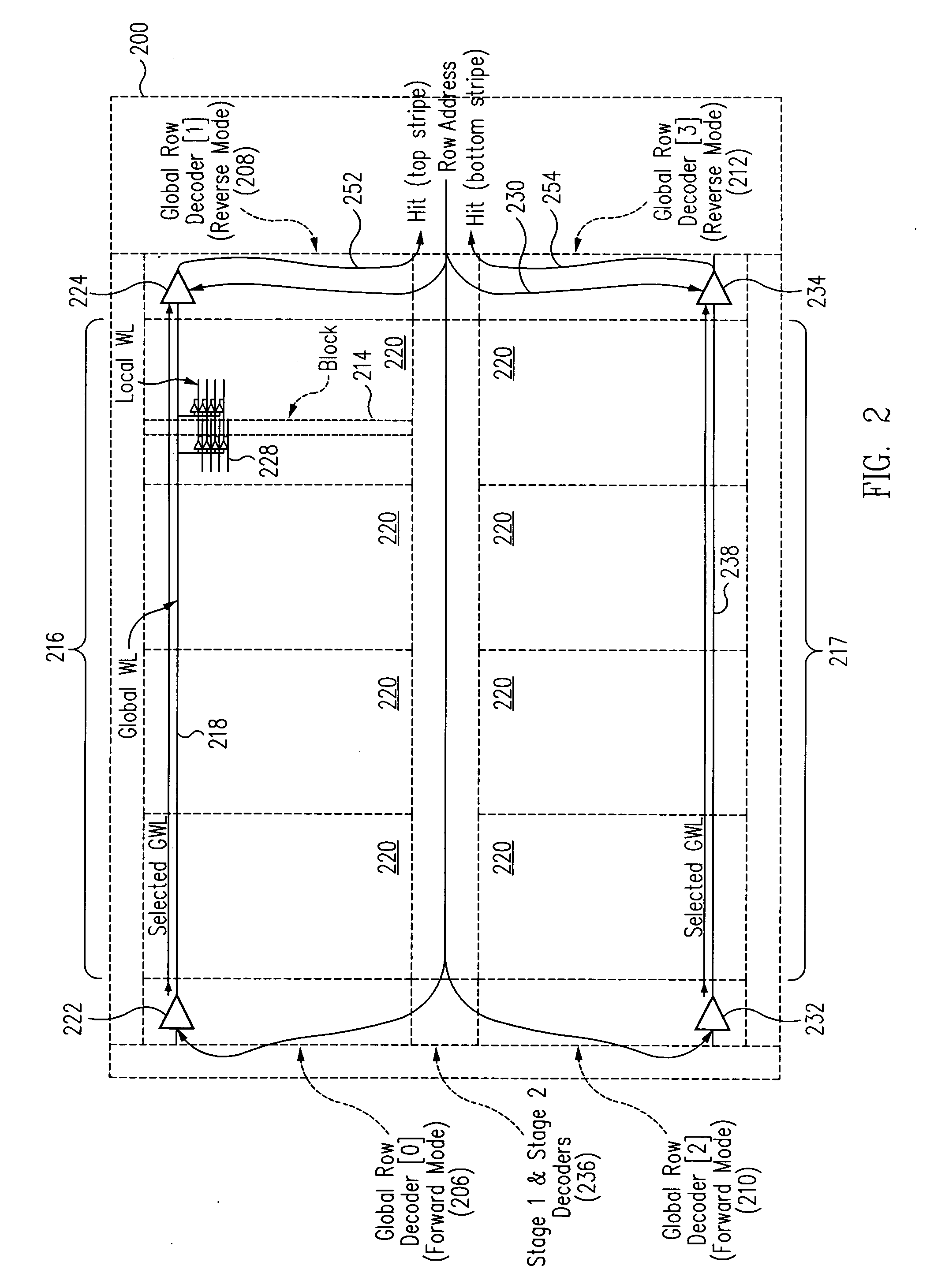
[0041] Referring now to FIG. 1, an exemplary integrated circuit 200 includes two memory arrays, one organized as part of an upper stripe 202, and the other organized as part of the lower stripe 204. The upper stripe 202 includes a memory array 216, a first dual-mode global word line decoder 206 disposed at the left side of memory array 216, and a second dual-mode global word line decoder 208 disposed at the right side of memory array 216. Both dual-mode decoders 206 and 208 are responsive to row addresses conveyed on row address lines 230.

[0042] The lower stripe 204 includes another memory array 217, a first dual-mode global word line decoder 210 disposed at the left side of memory array 217, and a second dual-mode global word line decoder 212 disposed at the right side of memory array 217. Both dual-mode decoders 210, 212 are also responsive to the row addresses 230.

[0043] In the upper memory array 202, the global word lines traverse across the entire memory array 216. One such ...


PUM


Abstract

In an embodiment of the invention an integrated circuit includes a memory array having a first plurality of decoded lines traversing across the memory array and a pair of dual-mode decoders, each decoder coupled to each of the plurality of decoded lines a respective location along said decoded lines, such as at opposite ends thereof. Both decoder circuits receive like address information. Normally both decoder circuits operate in a forward decode mode to decode the address information and drive a selected one of the decoded lines. During a test mode, one decoder is enabled in a reverse decode mode while the other decoder remains in a forward decode mode to verify proper decode operation and integrity of the decoded lines between the decoders.

Description

CROSS-REFERENCE TO RELATED APPLICATION(S) [0001] This application is related to co-pending U.S. application Ser. No. ______ {Attorney Docket No. 023-0033}, filed on even date herewith, entitled “Apparatus and Method for Hierarchical Decoding of Dense Memory Arrays Using Multiple Levels of Multiple-Headed Decoders” by Luca G. Fasoli and Kenneth K. So, which application is hereby incorporated by reference in its entirety.BACKGROUND [0002] 1. Field of the Invention [0003] The present invention relates to decoder circuits for integrated circuit memory arrays. [0004] 2. Description of the Related Art [0005] Semiconductor integrated circuits have progressively reduced their feature linewidths into the deep sub-micron regime. Moreover, recent developments in certain memory cell technologies have resulted in word lines and bit line having an extremely small pitch. For example, certain passive element memory cell arrays may be fabricated having word lines approaching the minimum feature size...

Claims


Application Information

Patent Timeline
Patent Type & Authority Applications(United States)
IPC IPC(8): H01L27/10G11C5/06
CPCG11C8/10
Inventor SO, KENNETH K.FASOLI, LUCA G.SCHEUERLEIN, ROY E.
Owner SANDISK TECH LLC
Why Eureka
Try Eureka