Bias circuit having reduced power-up delay

Inactive Publication Date: 2006-07-06
AGERE SYST INC
View PDF8 Cites 8 Cited by
  • Summary
  • Abstract
  • Description
  • Claims
  • Application Information

AI Technical Summary

Benefits of technology

[0007] The present invention meets the above-noted need by providing, in an illustrative embodiment, techniques for reducing current consumption in a bias circuit without significantly increasing a power-up delay of the bias circuit. The bias circuit is preferably operable in a power-down mode, wherein DC current in the circuit is substantially reduced to zero in response to a control signal applied thereto. In order to reduce power-up delay, the bias circuit includes a shunt circuit whi

Problems solved by technology

Although various techniques for reducing current consumption in a bias circuit may be known, standard bias circuits typically consume at least some measurable quantity of DC current, and, when multiplied by the large number of bias circuits that are often used in such applications, the overall DC power consumption attributable to these buffer circuits can be undesirably

Method used


Image

  • Bias circuit having reduced power-up delay
  • Bias circuit having reduced power-up delay
  • Bias circuit having reduced power-up delay

Examples


Example

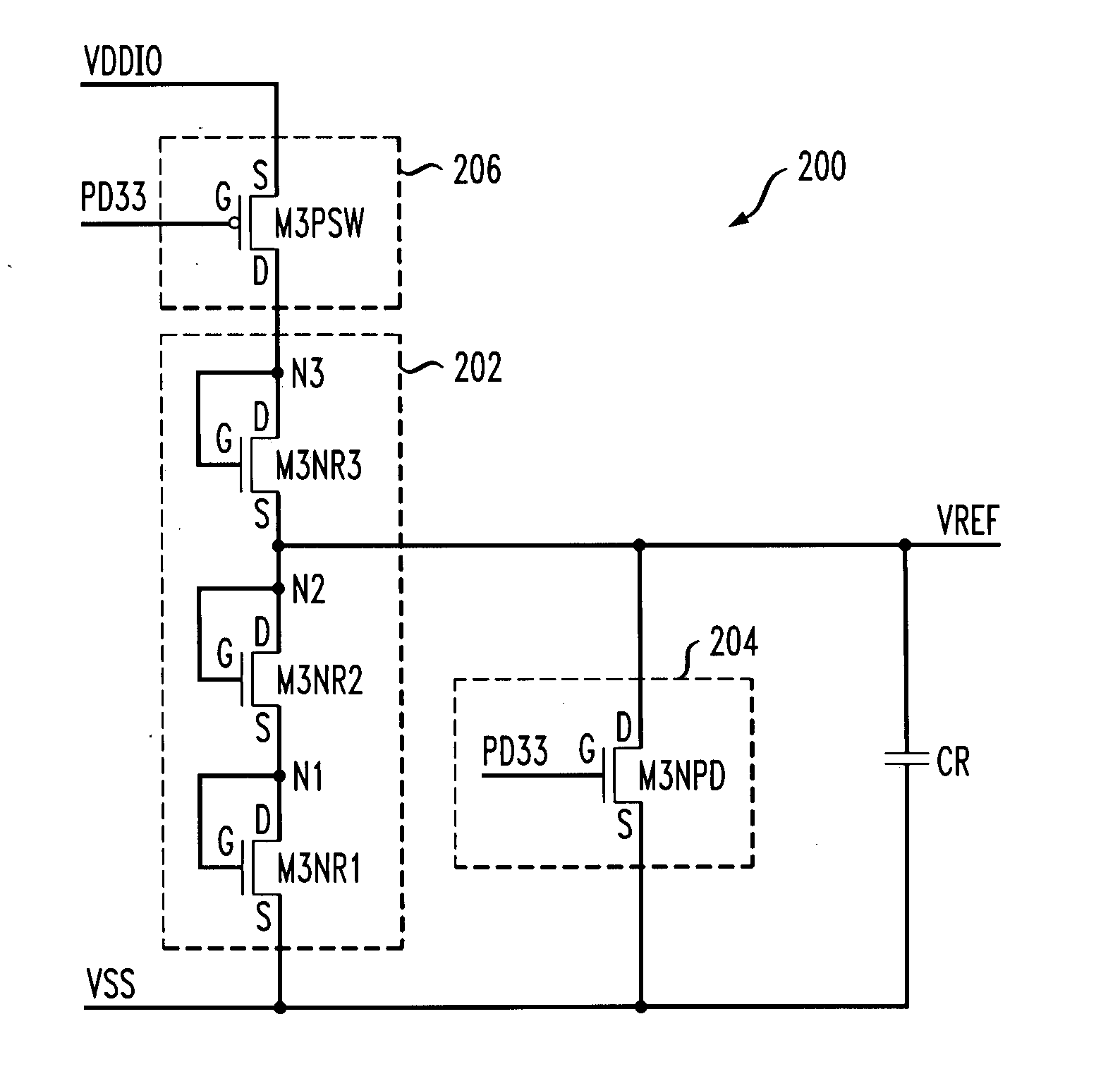
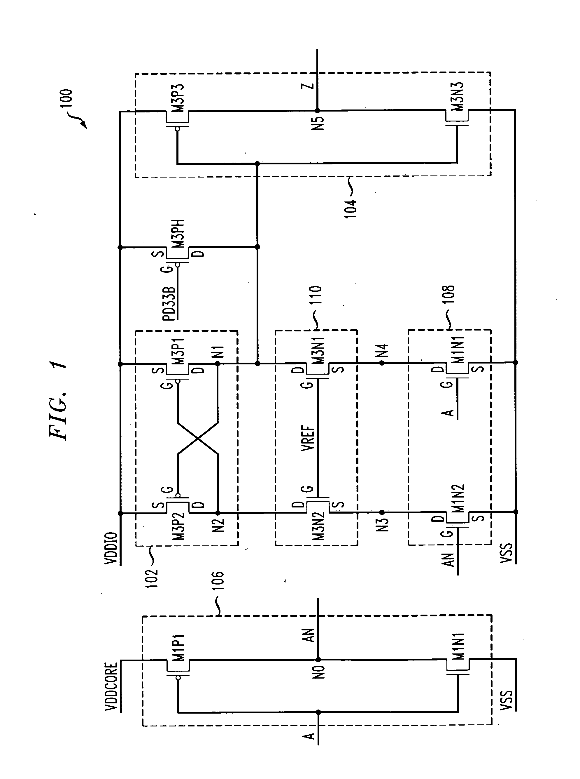
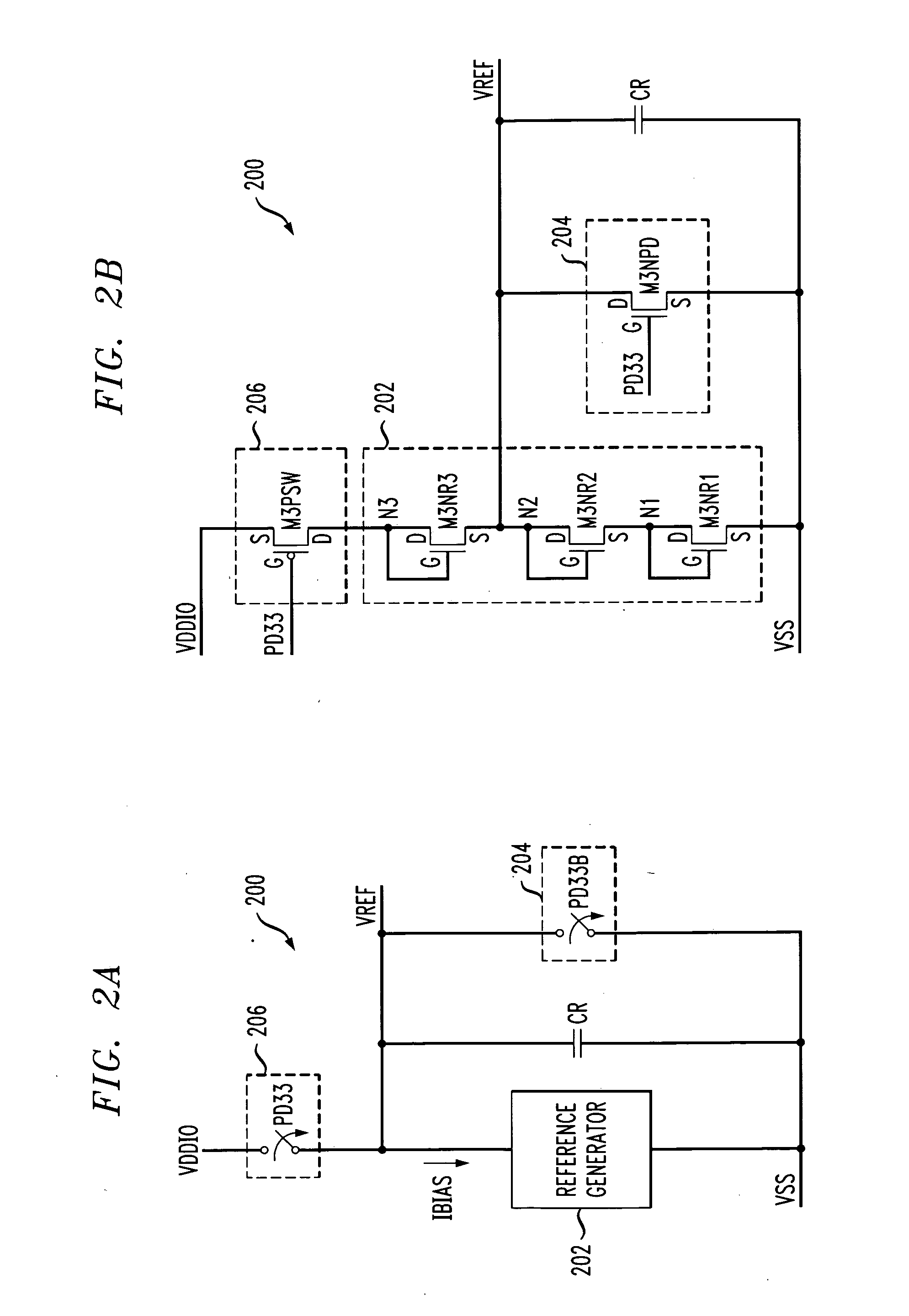
[0017] The present invention will be described herein in the context of illustrative bias circuits. It should be understood, however, that the present invention is not limited to these or any other particular bias circuit arrangements. Rather, the invention is more generally applicable to techniques for reducing DC current consumption in a bias circuit without significantly increasing power-up delay in the bias circuit. Furthermore, although described herein in the context of a voltage level translator circuit application, the techniques of the present invention may be extended to essentially any application requiring a bias circuit having reduced current consumption and without any significant power-up delay. Although implementations of the present invention are described herein with specific reference to P-type metal-oxide semiconductor (PMOS) and N-type metal-oxide semiconductor (NMOS) transistor devices, as may be formed using a complementary metal-oxide semiconductor (CMOS) fab...


PUM


Abstract

A bias circuit includes a reference generator for generating a bias signal at an output of the reference generator. The reference generator is selectively operable a first mode or a second mode in response to a first control signal applied to the reference generator, wherein in the first mode of operation, the reference generator is disabled, and in the second mode of operation, the reference generator is operative to generate the bias signal. The bias circuit further includes a shunt circuit connected to the reference generator. The shunt circuit is configured to provide a source of current to assist in charging the output of the reference generator to a quiescent operating level during the second mode of operation. The shunt circuit, in response to a second control signal applied thereto, is operable for a selected period time after the reference generator transitions from the first mode of operation to the second mode of operation.

Description

FIELD OF THE INVENTION [0001] The present invention relates generally to electronic circuits, and more particularly relates to bias circuits having reduced power consumption without a significant power-up delay. BACKGROUND OF THE INVENTION [0002] Bias circuits for generating a substantially fixed reference voltage and / or current are well known. In certain applications employing such bias circuits, particularly those applications involving portable devices, including wireless handsets, notebook computers and personal digital assistants (PDAs), reducing current consumption is a primary objective in order to extend the operating life of a battery often utilized in these devices. Therefore, it is desirable to minimize current consumption in the bias circuits as much as possible. [0003] Some portable devices may employ input / output (IO) buffer circuitry which runs on two or more different voltage levels. For instance, the IO buffer circuitry utilized with such portable devices may be con...

Claims


Application Information

Patent Timeline
IPC IPC(8): G05F1/10
CPCG05F3/205
Inventor BHATTACHARYA, DIPANKARKOTHANDARAMAN, MAKESHWARKRIZ, JOHN C.MORRIS, BERNARD L.SIMKO, JOSEPH E.
Owner AGERE SYST INC
Why Eureka
Try Eureka