Magnetic logic device and methods of manufacturing and operating the same

a logic device and magnetic field technology, applied in the field of magnetic logic devices and methods of manufacturing and operating the same, can solve the problem that the type of conventional logic devices cannot be changed, and achieve the effect of accurately controlling the magnetization direction, simple structure, and easy and simple manufacturing

Active Publication Date: 2006-07-06
SAMSUNG ELECTRONICS CO LTD
View PDF6 Cites 16 Cited by
  • Summary
  • Abstract
  • Description
  • Claims
  • Application Information

AI Technical Summary

Benefits of technology

[0030] The MLD of the present invention may be used as an AND gate or an OR gate by simply adjusting the magnetization direction of the upper magnetic layer of a magnetic tunnel junction (MTJ) cell. Therefore, the MLD may be selectively programmed according to the intended use thereof. In addition, the MLD has a simple structure and it can be easily and simply manufactured. Furthermore, since the magne...

Problems solved by technology

In addition, the determined type of the conventional logic device cannot be changed.
For example, a conventional...

Method used


Image

  • Magnetic logic device and methods of manufacturing and operating the same
  • Magnetic logic device and methods of manufacturing and operating the same
  • Magnetic logic device and methods of manufacturing and operating the same

Examples


Embodiment Construction

[0047] A magnetic logic device (MLD) and methods of manufacturing and operating the same according to exemplary embodiments of the present invention will now be described more fully with reference to the accompanying drawings. In the drawings, the thicknesses of layers and regions are exaggerated for clarity.

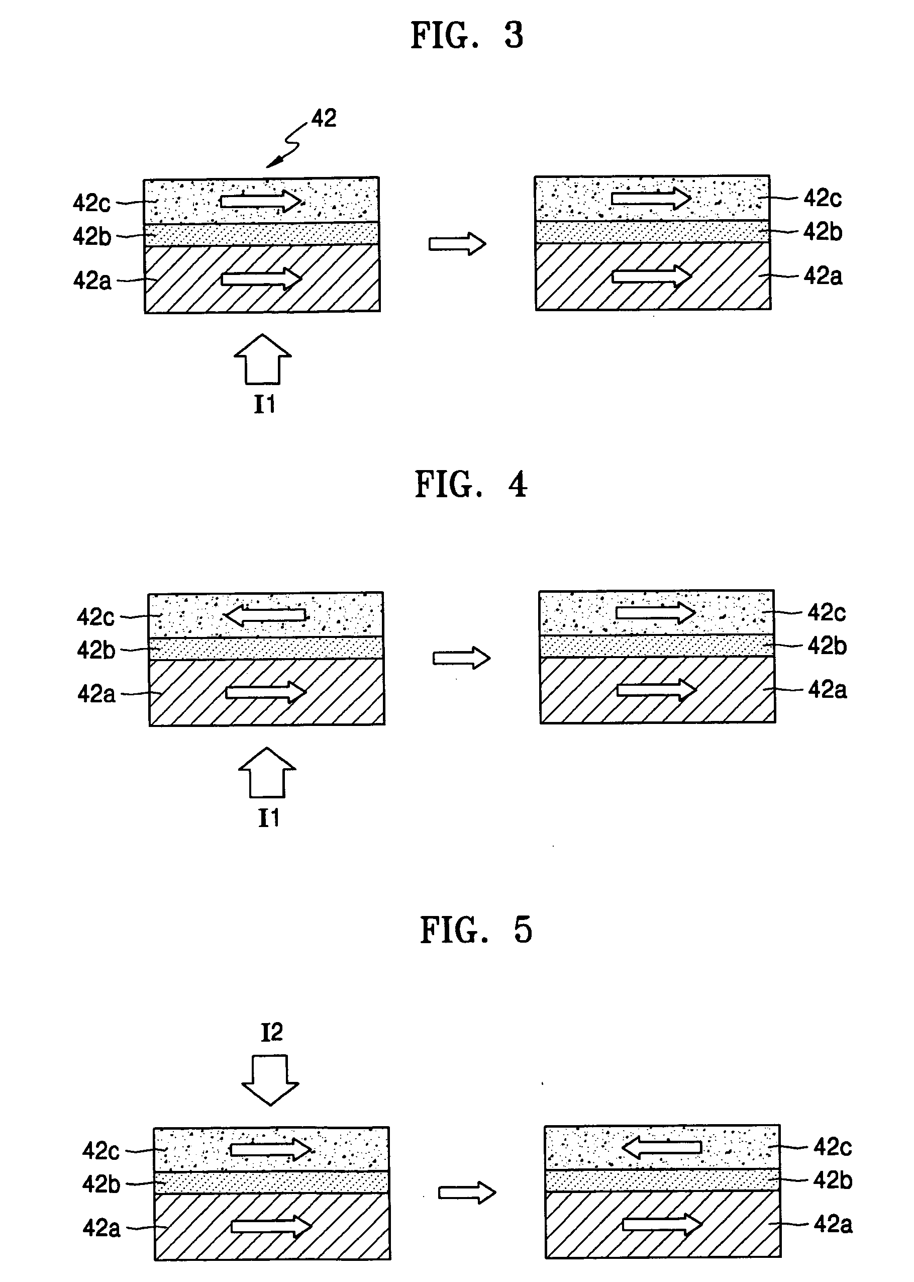
[0048] A magnetization direction of a magnetic material may be reversed by applying a magnetic field of a predetermined intensity to the magnetic material or by directly applying a spin polarization current of a critical value to the magnetic material.

[0049] An MLD according to exemplary embodiments of the present invention is realized by the direct application of a spin polarization current to the magnetic material.

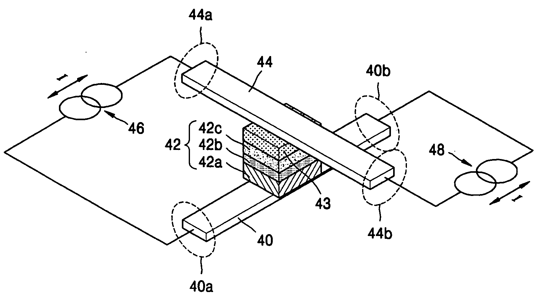
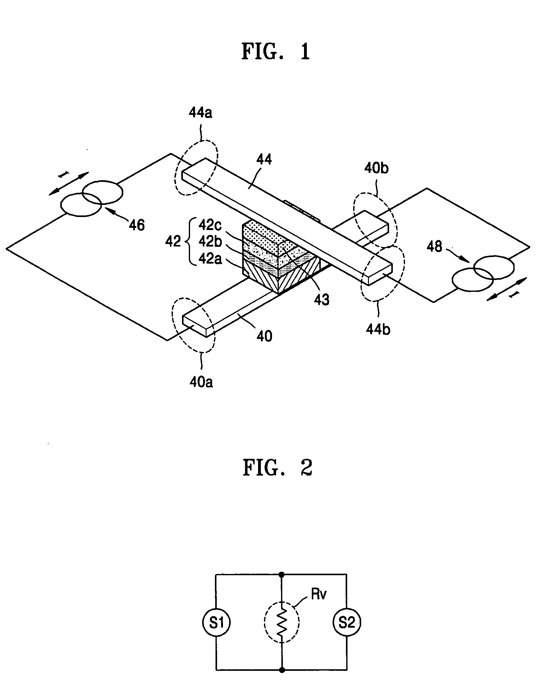
[0050]FIG. 1 is a three-dimensional schematic view illustrating an MLD according to an exemplary embodiment of the present invention.

[0051] Referring to FIG. 1, an MLD according to an exemplary embodiment of the present invention includes a first interconnection ...


PUM


Abstract

A magnetic logic device (MLD) and methods of manufacturing and operating an MLD are provided. The MLD includes: a first interconnection; a lower magnetic layer formed on the first interconnection, the lower magnetic layer having a magnetization direction fixed in a predetermined direction; a non-magnetic layer formed on the lower magnetic layer; an upper magnetic layer formed on the non-magnetic layer, the upper magnetic layer having a magnetization direction parallel or anti-parallel to the magnetization direction of the lower magnetic layer; and a second interconnection formed on the upper magnetic layer. A first current source is disposed between one end of the first interconnection and one end of the second interconnection and a second current source is disposed between the other end of the first interconnection and the other end of the second interconnection.

Description

CROSS-REFERENCE TO RELATED PATENT APPLICATION [0001] This application claims priority from Korean Patent Application No. 10-2004-0117010, filed on Dec. 30, 2004 in the Korean Intellectual Property Office, the disclosure of which is incorporated herein in its entirety by reference. BACKGROUND OF THE INVENTION [0002] 1. Field of the Invention [0003] The present invention relates to a semiconductor device, and more particularly, to a magnetic logic device and methods of manufacturing and operating the same. [0004] 2. Description of the Related Art [0005] Conventional logic devices, such as AND gates, OR gates, etc., consist of metal oxide semiconductor (MOS) transistors. Accordingly, the type of a conventional logic device is determined according to the structure of its MOS transistors. In addition, the determined type of the conventional logic device cannot be changed. For example, a conventional logic device initially manufactured as an AND gate can only be used as an AND gate and ca...

Claims


Application Information

Patent Timeline
IPC IPC(8): H01F5/00
CPCH01L43/08H03K19/16H10N50/10
Inventor KIM, SUNG-DONGKIM, EUN-SIKJUNG, JU-HWANKO, HYOUNG-SOOMIN, DONG-KIPARK, HONG-SIKHONG, SEUNG-BUM
Owner SAMSUNG ELECTRONICS CO LTD
Why Eureka
Try Eureka