

PIFA and RFID tag using the same
- Summary
- Abstract
- Description
- Claims
- Application Information
AI Technical Summary
Benefits of technology
Problems solved by technology
Method used
Image

Examples
first embodiment
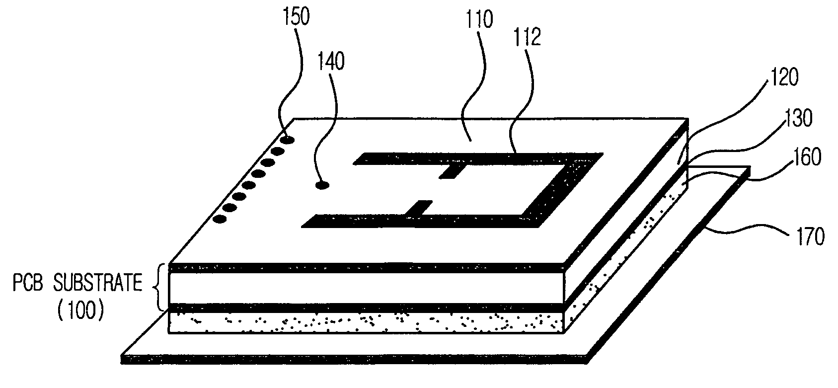
[0026]FIG. 3 is a perspective view showing a planar inverted-F antenna (PIFA) in accordance with the present invention, and FIG. 4 is a cross-sectional view showing the PIPA of FIG. 3. The PIFA of the present invention includes a radiation patch layer 110, a dielectric layer 120, a Co-Planar Waveguide (CPW) feeding layer 130, a feeding probe 140 and a short-circuit post 150.
[0027] The radiation patch layer 110 is formed on one side of a Printed Circuit Board (PCB) substrate 100. The PCB substrate 100 has conductive layers on the upper and lower sides of the dielectric layer 120. The radiation patch layer 110 is formed by etching the conductive layers of the PCB substrate 100. The radiation patch layer 110 radiates a Radio Frequency (RF) signal provided from the feeding probe 140 based on resonance in a resonant frequency of an antenna and. A U-type slot 112 is formed on the radiation patch layer 110. When the U-type slot 112 is formed on the radiation patch layer 110, a small antenn...
second embodiment
[0037]FIG. 7 is a perspective view of a PIFA in accordance with the present invention and FIG. 8 is a cross-sectional view of the PIFA shown in FIG. 7. The PIFA of the present invention includes a radiation patch layer 210, a first dielectric layer 220, a CPW feeding layer 230, a feeding probe 240, a short-circuit post 250 and a second dielectric layer 290.
[0038] The second embodiment further includes the second dielectric layer 290 in comparison with the first embodiment. The radiation patch layer 210 is formed by etching a conductive layer of a first PCB substrate 200a including the first dielectric layer 220 and a conductive layer. The CPW feeding layer 230 is formed by etching a conductive layer of a second PCB substrate 200b including the second dielectric layer 290 and a conductive layer. Since structures of the radiation patch layer 210, the CPW feeding layer 230, the feeding probe 240 and the short-circuit post 250 are the same as the structures of the radiation patch layer ...
PUM
 Abstract
Description
Claims
Application Information