

Method of forming a diffusion barrier layer using a TaSiN layer and method of forming a metal interconnection line using the same
- Summary
- Abstract
- Description
- Claims
- Application Information
AI Technical Summary
Benefits of technology
Problems solved by technology
Method used
Image

Examples
Embodiment Construction
[0021] An exemplary embodiment of the present invention will hereinafter be described in detail with reference to the accompanying drawings.
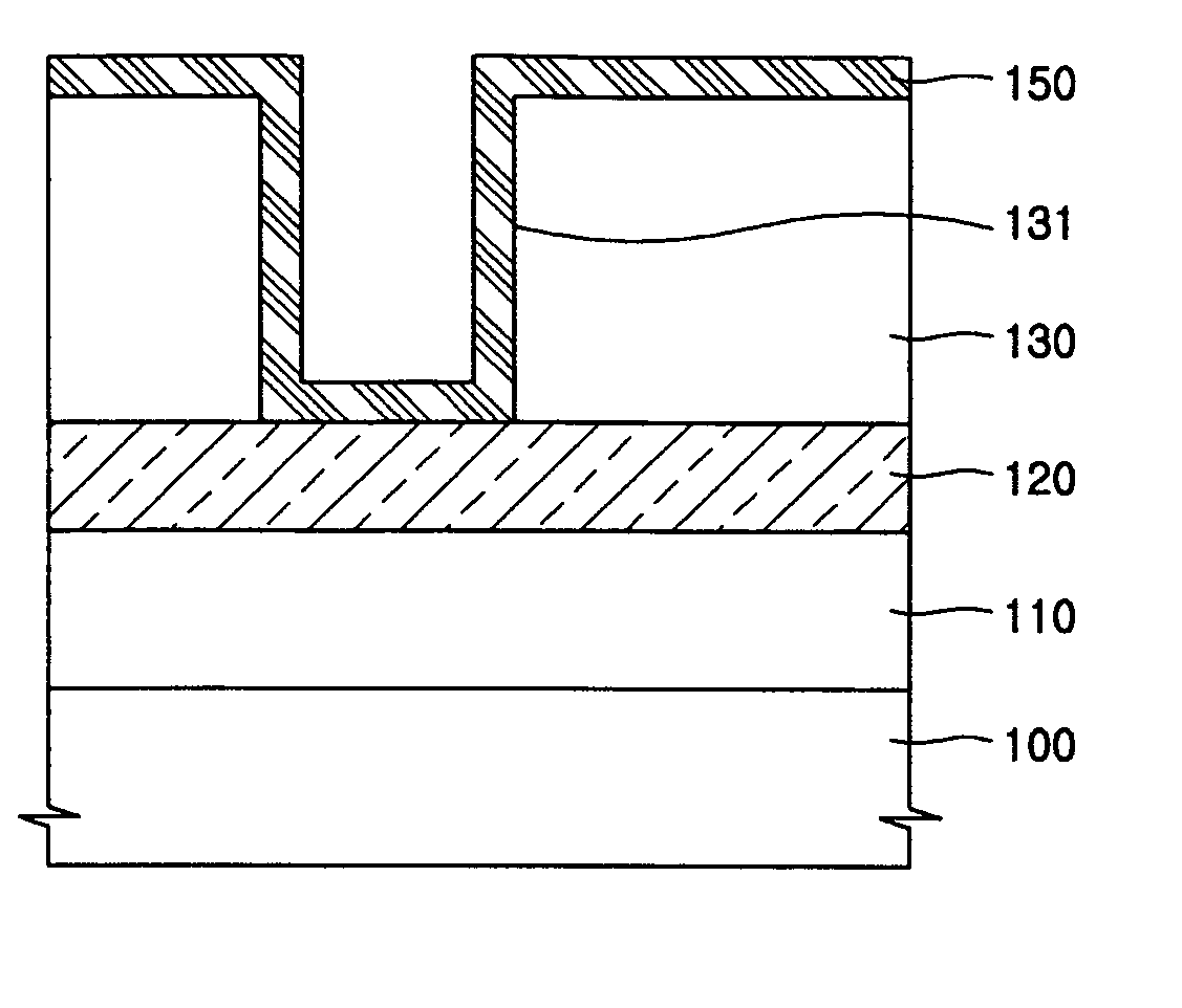
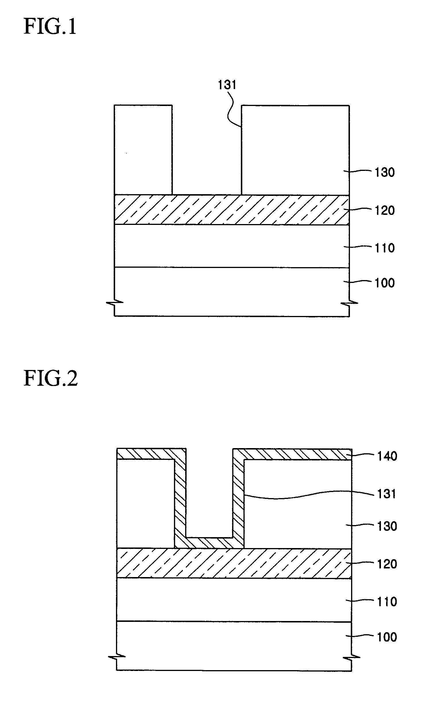
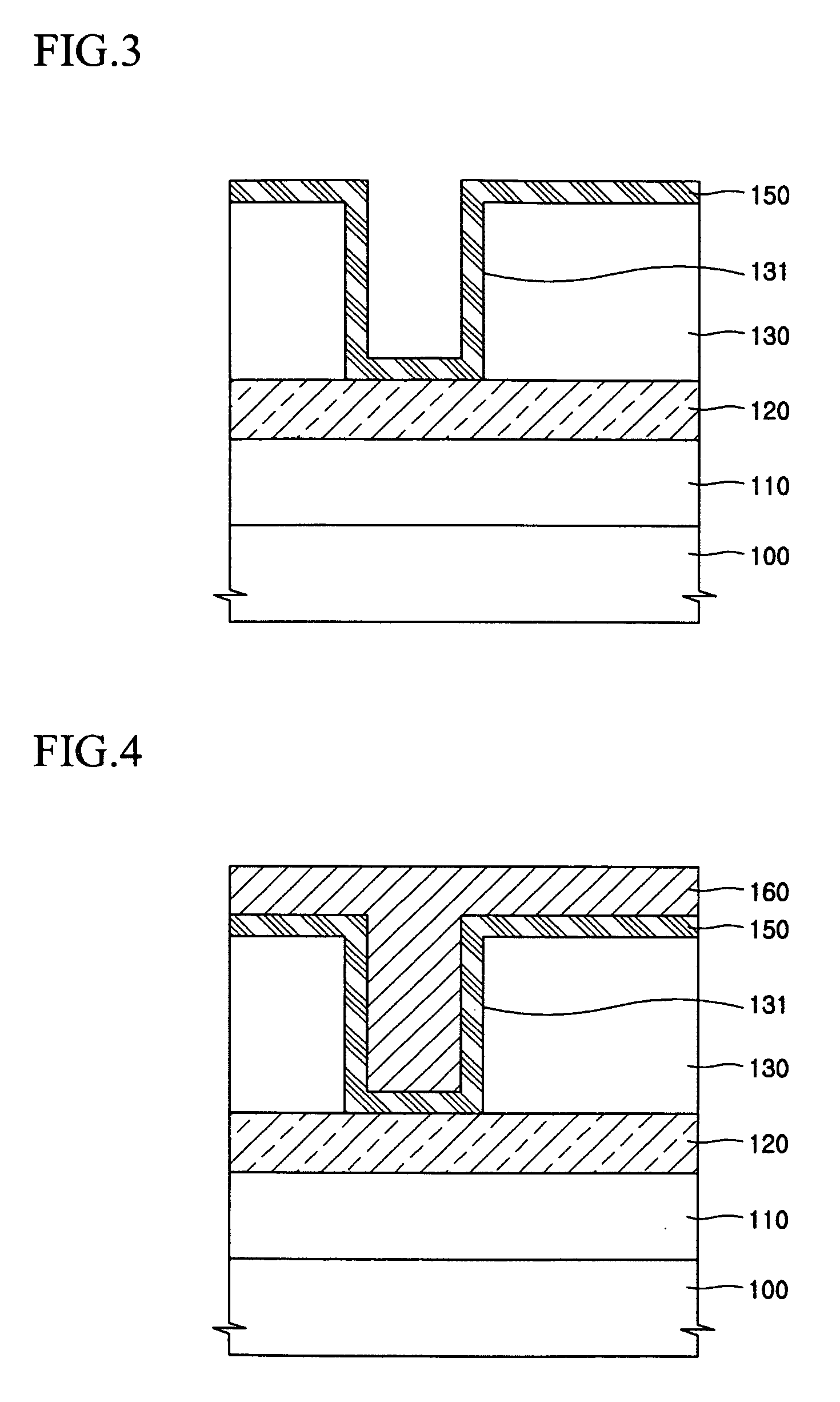
[0022]FIG. 1 to FIG. 4 are cross-sectional views showing a method of forming a diffusion barrier layer comprising a TaSiN layer and a method of forming a metal interconnection line including the same according to an exemplary embodiment of the present invention.
[0023] Referring to FIG. 1, an insulation layer 110 and a first metal line layer 120 are sequentially formed on a semiconductor substrate 100. The insulation layer 110 may be an interlayer insulation layer (e.g., an insulation layer between a polysilicon layer and a metallization layer) or an intermetal insulation layer (e.g., an insulation layer between two adjacent metallization layer). When the insulation layer 110 is an intermetal insulation layer, another lower-level metal line layer (not shown) may be located below the intermetal insulation layer. Subsequently, in this latter embo...
PUM
 Abstract
Description
Claims
Application Information