Semiconductor producing device and semiconductor producing method

Inactive Publication Date: 2006-07-13
KOKUSA ELECTRIC CO LTD
View PDF12 Cites 224 Cited by
  • Summary
  • Abstract
  • Description
  • Claims
  • Application Information

AI Technical Summary

Benefits of technology

[0011] Damage to the high frequency electrode is therefore prevented even if a difference in the

Problems solved by technology

However, this type of semiconductor producing device has the problem of low heating efficiency in the heater.
The above described semiconductor producing device has the problem that during hea

Method used


Image

  • Semiconductor producing device and semiconductor producing method
  • Semiconductor producing device and semiconductor producing method
  • Semiconductor producing device and semiconductor producing method

Examples


second embodiment

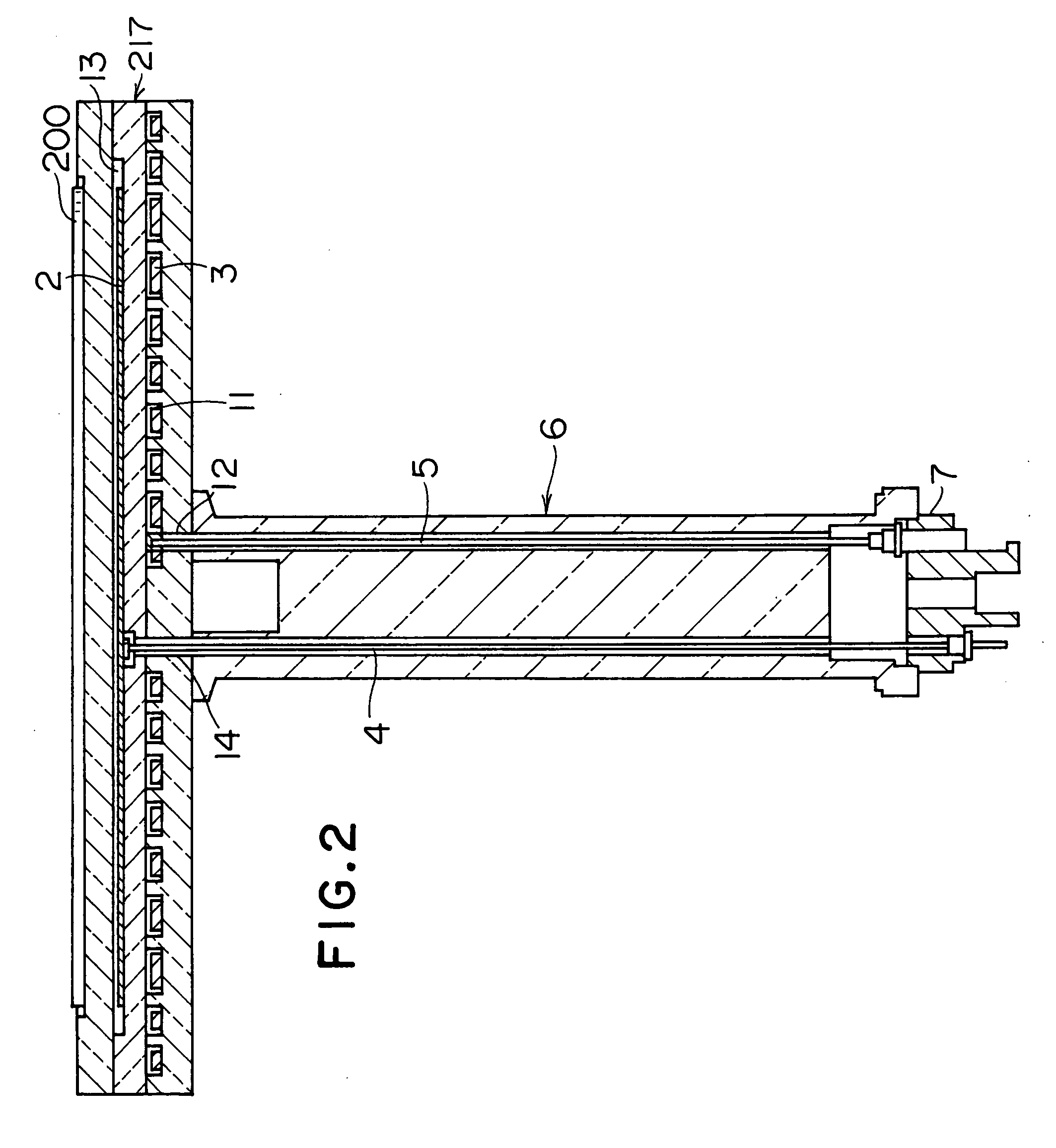
[0049]FIG. 3 is a frontal cross sectional view of a section of the susceptor of the MMT device of the present invention. FIG. 4 is a plan view taken along line IV-IV of FIG. 3.

[0050] The susceptor 217 of this embodiment is formed from quartz or aluminum nitride. Preferably, quartz is utilized since a large temperature differential occurs within the susceptor 217 in the high temperature region for example of 500° C. or more, and the strength must be maintained. Incidentally, neither quartz or aluminum nitride do not cause metallic contamination effects on the wafer 200 which is the substrate for processing.

[0051] The susceptor 217 of the present embodiment is comprised of a first susceptor member 1a as a lid, and a second susceptor member 1b as the main piece. A groove 8 is formed in a lattice shape in the upper surface of the second susceptor member 1b. A high frequency electrode 2a in a mesh shape and serving as the second electrode is installed on the groove 8 and the first susce...

third embodiment

[0059]FIG. 5 is a partial cross sectional front view showing the susceptor of the MMT device of the present invention.

[0060] The overall structure of the MMT device of this embodiment and the schematic structure of the susceptor are the same as the previously described MMT device and susceptor.

[0061] The susceptor 217 of this embodiment is comprised of an upper stage susceptor member 1c and intermediate stage susceptor member 1d and lower stage susceptor member le and a mounting susceptor member if. The material is overall quartz. The high frequency electrode 2a serving as the second electrode is installed inside the upper stage susceptor member 1c.

[0062] The mounting susceptor member 1f is fabricated separately from the upper stage susceptor member 1c and clamped air-tight by adhesive material or heat weld. The mounting susceptor member 1f may however be formed as one piece with the upper stage susceptor member 1c.

[0063] An upper side cavity 10a is formed on the upper surface of...


PUM

PropertyMeasurementUnit
Poweraaaaaaaaaa

Abstract

A tubular electrode (215) and a tubular magnet (216) are installed on an external section of a processing furnace (202) for an MMT device. A susceptor (217) for holding a wafer (200) is installed inside a processing chamber (201) of the processing furnace. A gate valve (244) for conveying the wafer into and out of the processing chamber; and a shower head (236) for spraying processing gas in a shower onto the wafer, are installed inside the processing furnace. A high frequency electrode (2) and a heater (3) are installed inside the susceptor (217) with a clearance between them and the walls forming the space. The clearances formed between the walls forming the space in the susceptor and the high frequency electrode and the heater prevent damage to the high frequency electrode and the heater even if a thermal expansion differential occurs between the high frequency electrode, the heater and the susceptor.

Description

TECHNICAL FIELD [0001] The present invention relates to a semiconductor producing device for plasma processing of substrates. BACKGROUND ART [0002] In semiconductor producing devices of this type in the prior art, the substrate for processing is loaded onto a substrate holding means installed within a vacuum container, a processing gas is supplied while the vacuum container is evacuated, and plasma discharge is generated in the processing gas by plasma generating sources of different types to subject the substrate to plasma processing using the processing gas activated by the plasma discharge. [0003] A heater and high frequency electrode are installed within the substrate holding means in accordance with the necessary of plasma processing. The heater performs the heating of the substrate for processing. The high frequency electrode to which a high frequency voltage is applied applies a bias voltage to the substrate. This high frequency electrode is also utilized as an electrode for ...

Claims


Application Information

Patent Timeline
IPC IPC(8): C23F1/00H01L21/302H01L21/00
CPCH01J37/32082Y10T279/23H01L21/67103H01J2237/2001H01L21/68792H01L21/68757H01J37/32724H05B3/143H05B3/283
Inventor KASANAMI, KATSUHISAMIYATA, TOSHIMITSUISHISAKA, MITSUNORI
Owner KOKUSA ELECTRIC CO LTD
Why Eureka
Try Eureka