Semiconductor light emitting device, method of manufacturing the same, and lighting apparatus and display apparatus using the same

a technology of semiconductors and light emitting devices, which is applied in the direction of semiconductor/solid-state device details, lighting and heating apparatus, solid-state devices, etc., can solve the problems of reducing positioning accuracy and bonding strength, destroying depressions, and not being very realistic, and achieve excellent light emitting efficiency.

Active Publication Date: 2006-07-13
SIGNIFY HLDG BV
View PDF4 Cites 74 Cited by
  • Summary
  • Abstract
  • Description
  • Claims
  • Application Information

AI Technical Summary

Benefits of technology

[0008] In order to solve the above noted problems, the present invention aims to provide a semiconductor light emitting device that may be firmly attached to a substrate with maintaining excellent light emitting efficiency, and a manufacturing method of the same, and a lighting apparatus and a display apparatus using the same.

Problems solved by technology

However, this solution is not very realistic due to current issues regarding production cost and heat dissipation in driving when LEDs are mounted in high density.
However, mounting bare chips having depressions on the light extracting surface using the flip-chip bonding often causes problems such as decreases in positioning accuracy and bonding strength, and destruction of the depressions.
The same kind of problems also occur in display apparatuses having bare chips.

Method used


Image

  • Semiconductor light emitting device, method of manufacturing the same, and lighting apparatus and display apparatus using the same
  • Semiconductor light emitting device, method of manufacturing the same, and lighting apparatus and display apparatus using the same
  • Semiconductor light emitting device, method of manufacturing the same, and lighting apparatus and display apparatus using the same

Examples


first embodiment

[0062] In a first embodiment, an LED bare chip (hereinafter referred to as the LED chip) 1 is used as an example of semiconductor light emitting devices.

[Structure of LED Chip 1]

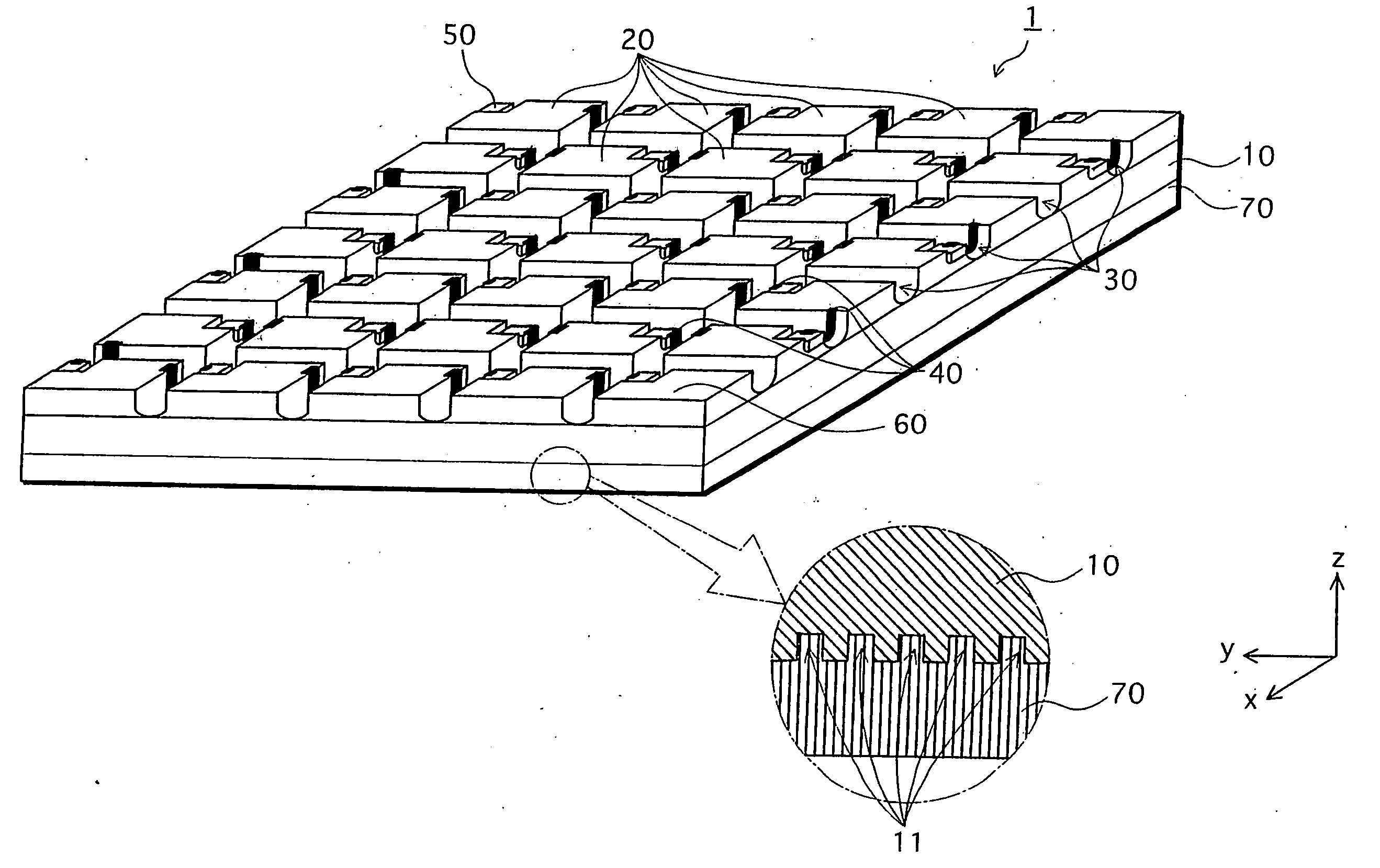
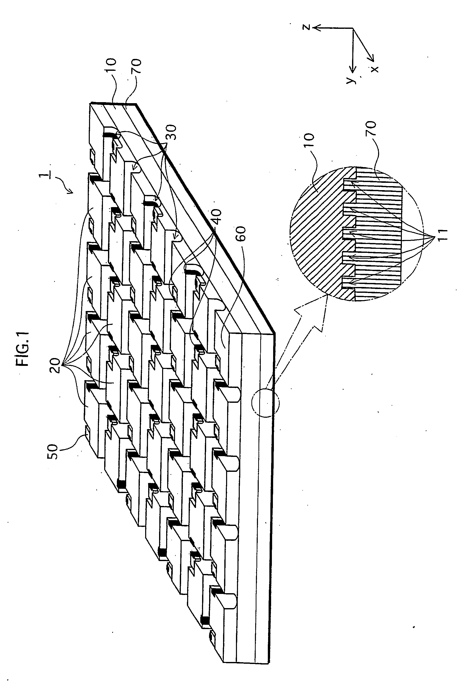
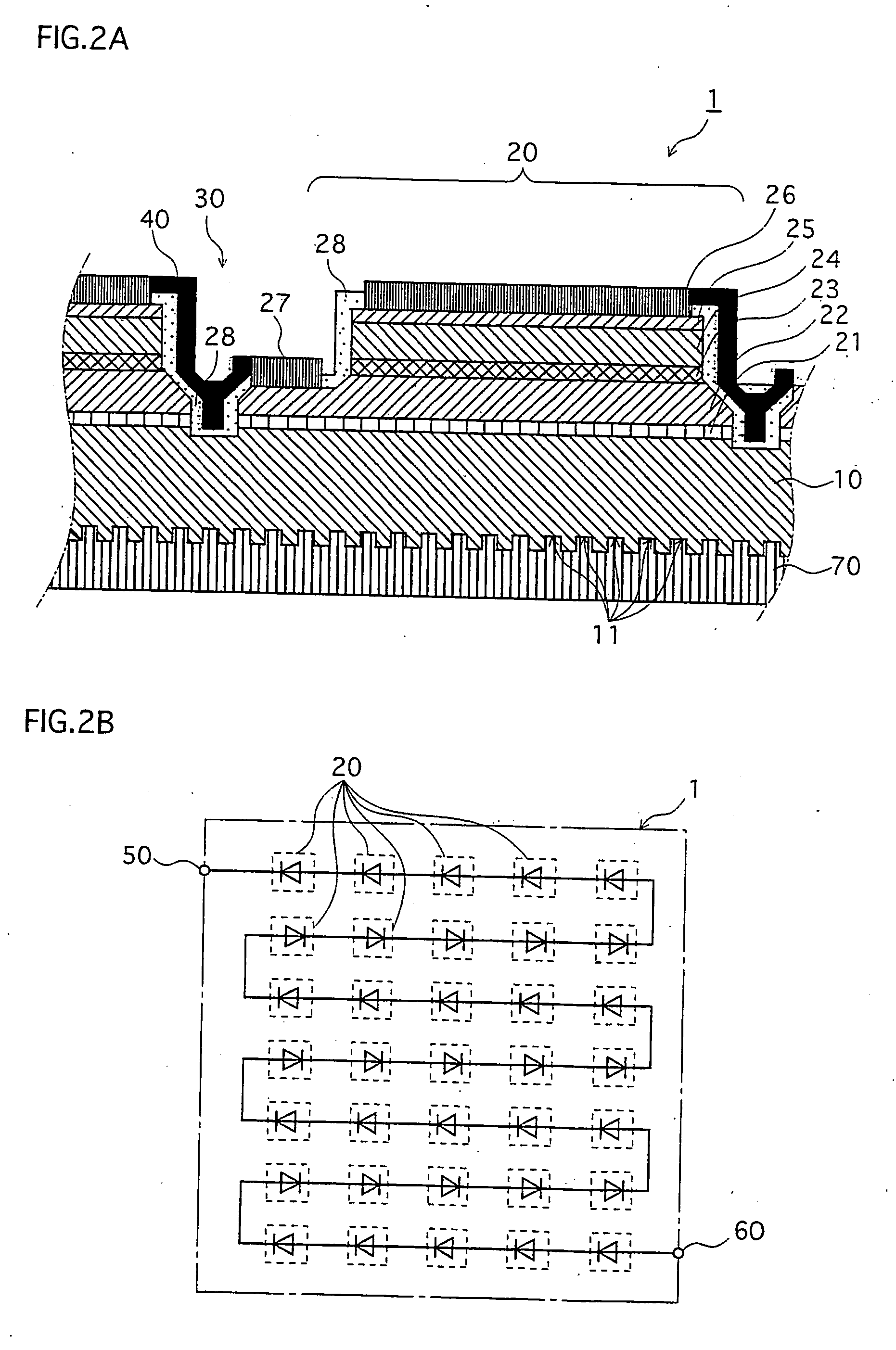
[0063] The LED chip 1 is explained with reference to FIGS. 1 and 2. FIG. 1 shows a perspective view. FIG. 2A shows a partial sectional view, and FIG. 2B shows a circuit wiring diagram, of the LED chip 1.

[0064] As shown by FIG. 1, the LED chip 1 is such that plural light-emitting elements 20 are formed on a non-doped GaN substrate 10. The light emitting elements 20 are disposed on the substrate 10 in a matrix of 7×5 in x and y directions respectively to form total 35 regions on the substrate. A size of one light emitting element 20 is 285 μm in x direction, and 400 μm in y direction. A size of the LED chip 1 is 2 mm×2 mm, for example.

[0065] Each of the light emitting elements 20 on the LED chip 1 constitutes a diode structure, and is separated from other light emitting elements 20 by separation grooves 30...

second embodiment

[0125] In a second embodiment, a LED chip 3 as an example of the semiconductor light emitting device is explained.

[Structure of LED Chip 3]

[0126] The LED chip 3 according to the present embodiment has a similar appearance with the LED chip 1 shown in FIG. 1. Specifically, light emitting elements 320 each having a size of 285 μm×400 μm are disposed in a matrix of 7×5, and a size of the LED chip 3 is 2×2 mm. Below, a structure of the LED chip 3 is explained focusing on differences from the LED chip 1, with reference to FIG. 11. FIG. 11A illustrates a partial sectional view of the LED chip 3, and FIG. 11B illustrates a top view of the LED chip 3 without a membrane 370, which will be explained later.

[0127] As shown in FIG. 11A, the LED chip 3 is formed in a manner that an AlGaN buffer layer 321 (30 nm thick), an n-Al0.1Ga0.9N clad layer 322 (Si doped 3×10 cm−1, 1.5 μm thick), an In0.03Ga0.97N / Al0.05Ga0.95N×5 luminous layer 323 (In0.03Ga0.97N is 3 nm thick, and Al0.05Ga0.95N is 5 nm t...

example 1

[0134] A combination of blue phosphor material, green phosphor material, and red phosphor material, emitting blue light, green light, and red light, respectively when excited by the near-ultraviolet light.


PUM


Abstract

The present invention aims to provide a semiconductor light emitting device (1) that may be firmly attached to a substrate with maintaining excellent light emitting efficiency, and a manufacturing method of the same, and a lighting apparatus and a display apparatus using the same. In order to achieve the above object, the semiconductor light emitting device (1) according to the present invention includes a luminous layer (23), a light transmission layer (10) disposed over a main surface of the luminous layer (23), and having depressions (11) on a surface facing away from the luminous layer (23), and a transmission membrane (70) disposed on the light transmission layer (10) so as to follow contours of the depressions, and light from the luminous layer (23) is irradiated so as to pass through the light transmission layer (10) and the transmission membrane (70).

Description

TECHNICAL FIELD [0001] The present invention relates to a semiconductor light emitting device and a method of manufacturing the same, as well as a lighting apparatus and a display apparatus using the same. BACKGROUND ART [0002] Lighting apparatuses with light emitting diodes (LEDs) have been gaining attention as a new light source because of excellent properties in terms of light emitting efficiency and longevity in comparison with incandescent lamps or halogen lamps. In order to improve light output of this kind of lighting apparatus, a quick solution is to mount LEDs in high density. However, this solution is not very realistic due to current issues regarding production cost and heat dissipation in driving when LEDs are mounted in high density. A more realistic solution in order to enhance the light output is to make luminous efficiency of an LED as high as possible. Various attempts have been made to this end, and two key parameters in making such attempts are Internal Quantum Ef...

Claims


Application Information

Patent Timeline
Patent Type & Authority Applications(United States)
IPC IPC(8): H01L33/00F21K99/00H01L25/075H01L27/15
CPCH01L23/16H01L25/0753H01L27/156H01L33/20H01L2224/48091H01L2224/73265H01L2924/00
Inventor NAGAI, HIDEO
Owner SIGNIFY HLDG BV
Why Eureka
Try Eureka