Optical-pickup slider, manufacturing method thereof, probe and manufacturing method thereof, and probe array and manufacturing method thereof

a technology of optical pick-up slider and manufacturing method, which is applied in the manufacture of head surfaces, instruments, applications, etc., can solve the problems of not being able to disclose the method of obtaining this aperture, not being able to form a very small aperture, and being difficult to stop etching just in time, etc., to achieve high repeatability and high accuracy

Inactive Publication Date: 2006-07-13
RICOH KK
View PDF13 Cites 11 Cited by
  • Summary
  • Abstract
  • Description
  • Claims
  • Application Information

AI Technical Summary

Benefits of technology

[0026] An object of the present invention is to provide an optical-pickup slider and a manufacturing method thereof in which it is possible to make an aperture, which is not likely to be destroyed, by a single time of etching, with high accuracy and high repeatability.
[0027] Further, in an actual optical pickup-head slider 10, a ski 51 as shown in FIG. 10A or a pad 52 as shown in FIG. 10B is provided, for a purpose of smooth floating of the head without adhering a recording medium. Another object of the present invention is to make the ski 51 or pad 52 with high accuracy and high repeatability.

Problems solved by technology

However, this document does not disclose how to obtain this aperture, concretely.
The slider has a thickness of millimeters in general, and it is not easy to form a very small aperture equal to or smaller than 200 nm through this thickness.
Accordingly, it is actually very difficult to stop etching just in time so as to achieve an opening dimension of tens of nanometers from a previously measured etching speed and a substrate thickness.
Thereby, in this condition, it is not possible that the opening approaches a recording medium to a distance of tens of nanometers.
However, because a thickness of a portion having the opening is on the order of 10 μm, it is likely to be destroyed when or after the fringe is removed.
However, in this case, as shown in FIG. 6E or FIG. 7E, when photo resist 74 is coated, because a level difference of hundreds of microns exists from a surrounding fringe portion, it is not possible to coat the photo resist uniformly, and to form the pattern of silicon oxide with high accuracy.
However, the width of each recess 1001 involves an error on the order of approximately 10 nm due to variation in mechanical accuracy even when an electronic-beam exposing device is used.
Accordingly, it is not possible to make uniform heights of respective projections of a projection-type probe array made by using the recess array 1000.
Further, when a single-projection probe is made, the above-mentioned problem involved in manufacturing of a projection-type probe array does not arise.
However, the following problems arise.
However, a planarity of the bottom surface 3002 of the recess 3001 made in the related art is far from reaching this.
Accordingly, it is not possible to make a satisfactory projection-type probe by the related art.
In order to cope therewith, an opening width W may be made to change correspondingly to a variation of a depth H. However, it is not possible to measure a depth H precisely.
Furthermore, it is not possible to change a dimension of a photo mask, actually.
Thus, even manufacturing of a single-projection probe which does not need consideration of making uniform heights of a plurality of projections involves problems on dimension accuracy in the related art.

Method used


Image

  • Optical-pickup slider, manufacturing method thereof, probe and manufacturing method thereof, and probe array and manufacturing method thereof
  • Optical-pickup slider, manufacturing method thereof, probe and manufacturing method thereof, and probe array and manufacturing method thereof
  • Optical-pickup slider, manufacturing method thereof, probe and manufacturing method thereof, and probe array and manufacturing method thereof

Examples


first embodiment

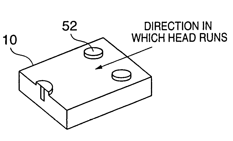
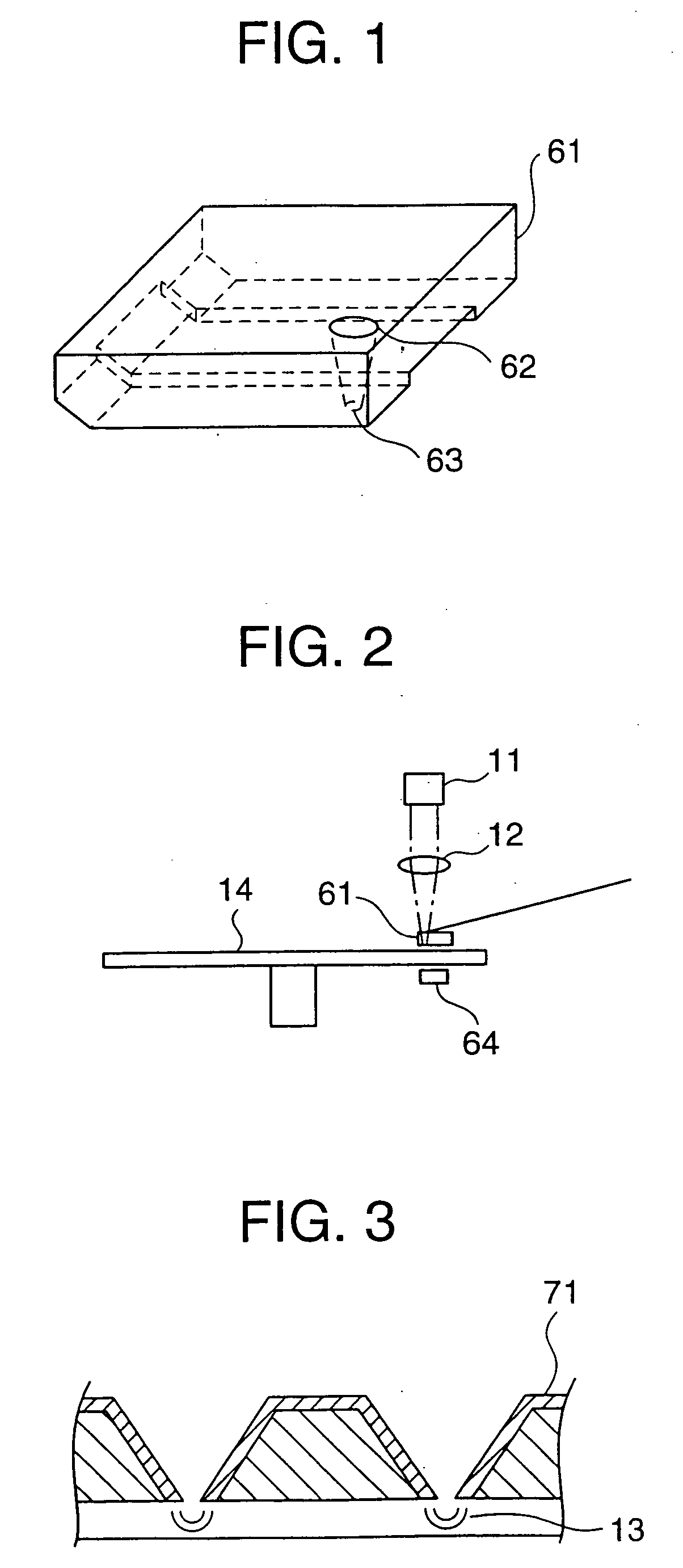
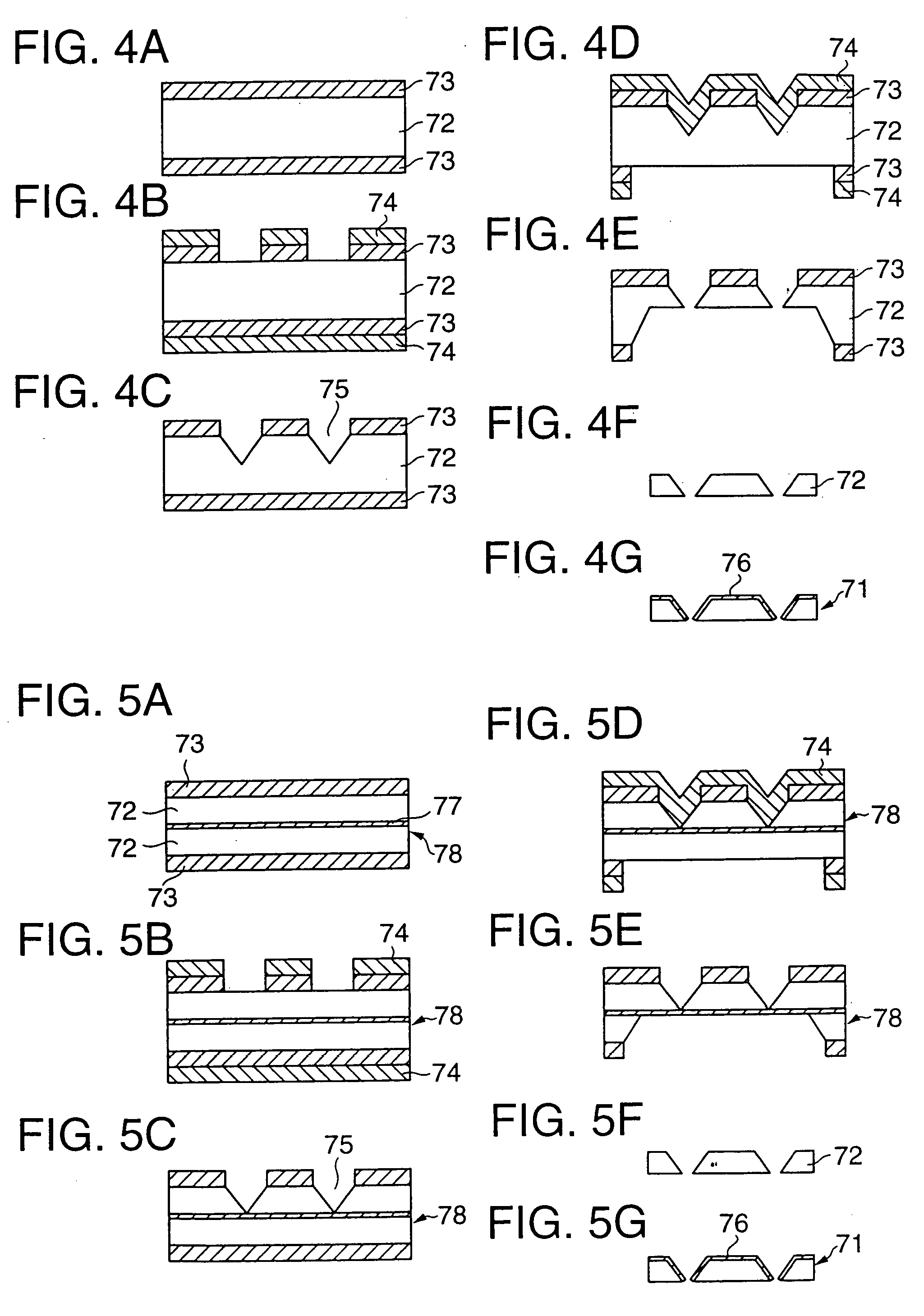
[0227]FIGS. 11A through 11F show a process of manufacturing an optical pickup-head slider (being simply referred to as a slider, hereinafter) in the present invention. As shown in FIG. 11A, a so-called SOI substrate obtained as a result of an SiO2 layer 3 having a thickness of approximately 1 μm and a single-crystal Si (silicon) layer 4 having a (100) plane on the top side thereof and having a thickness of approximately 10 μm being layered on a single-crystal Si substrate 2 having a thickness of hundreds of microns is used as a substrate 1. On the surface of the single-crystal Si layer 4, an SiO2 layer 5 having a thickness of hundreds of nanometers is layered. A portion of the SiO2 layer 5 at which an opening is to be made is removed by photolithographic etching as shown in FIG. 11A. This portion of the SiO2 layer 5 to be removed has a dimension determined such that an opening dimension of a bottom surface of a hole in an interface between the single-crystal Si layer 4 and SiO2 laye...

second embodiment

[0234] In the above-described embodiment, an SOI substrate is used as a substrate 1. A second embodiment in which a substrate other than an SOI substrate is used will now be described.

[0235] In the second embodiment, as shown in FIG. 13A, a substrate 21 is obtained as a result of an n-type Si layer 23 having a (100) plane on the top side thereof and having a thickness of tens of microns being layered on a p-type Si substrate 22 having a thickness of hundreds of microns, the substrate 21 having an SiO2 layer 24 having a thickness of hundreds of nanometers on the surface of the n-type Si layer 23. A portion of the SiO2 layer 24 at which an opening is formed is removed by photolithographic etching, as shown in FIG. 13A. A dimension of this portion of the SiO2 layer 24 to be removed is determined such that an aperture dimension of a bottom surface of a hole in an interface between the n-type Si layer 23 and p-type Si layer 22 will be in the range of tens of nanometers to hundreds of nan...

third embodiment

[0239] A third embodiment in which a substrate obtained as a result of a low-concentration p-type or n-type Si layer being layered on a high-concentration p-type or n-type Si substrate is used will now be described making reference to a process chart shown in FIGS. 15A through 15E.

[0240] As shown in FIG. 15A, a substrate 31 is obtained as a result of a low-concentration p-type or n-type Si layer 33 having a (100) plane on the top side thereof and having a thickness of tens of microns being layered on a high-concentration p-type or n-type Si substrate 32 having a thickness of hundreds of microns, the substrate 31 having an SiO2 layer 34 having a thickness of hundreds of nanometers on the surface of the low-concentration Si layer 33. Here, it is important that respective impurity concentrations of the high-concentration Si substrate 32 and low-concentration Si layer 33 are high and low. Any combinations of p-type Si and n-type Si are possible, however, it is preferable that the low-co...


PUM

PropertyMeasurementUnit
diameteraaaaaaaaaa
thicknessaaaaaaaaaa
thicknessaaaaaaaaaa

Abstract

An optical-pickup slider is characterized in that a light-transmitting-property substrate is bonded to a surface of a layer having a tapered through hole, on which surface a larger opening of the tapered through hole exists. Thereby, it is possible to prevent the layer having an aperture from being destroyed. A method of manufacturing the optical-pickup slider comprises the steps of a) making a tapered through hole in a layer layered on a first substrate and having a thickness smaller than that of the first substrate; and, after bonding a light-transmitting-property substrate to a surface of the layer, removing the first substrate so as to expose an aperture at a tip of the tapered through hole.

Description

[0001] This application is a Divisional Application of application Ser. No. 10 / 720,444, filed Nov. 25, 2003, which is a divisional of application Ser. No. 09 / 585,428, filed Jun. 2, 2000, now U.S. Pat. No. 6,680,900, issued Jan. 20, 2004, the entire disclosures of which are hereby incorporated by reference. BACKGROUND OF THE INVENTION [0002] 1. Field of the Invention [0003] The present invention generally relates to an optical-pickup slider using an optical near-field and floating a predetermined distance above a high-density recording medium by an air flow, and a manufacturing method thereof. [0004] The present invention further relates to a probe suitable for gathering incident light and emitting it to a sample to be measured or a recording medium for example, and a manufacturing method thereof, a probe array and a manufacturing method thereof, and, in more detail, to a probe which can gather incident light and generate an optical near-field and / or propagation light, a manufacturin...

Claims


Application Information

Patent Timeline
Patent Type & Authority Applications(United States)
IPC IPC(8): G11B15/64B29D11/00G11B7/12G11B7/135G11B7/22
CPCB82Y10/00G01Q60/22G11B5/6005G11B7/1203G11B7/1387Y10T29/49048Y10T29/4902Y10T29/49046Y10T29/49032Y10T29/49002Y10T29/49041G11B7/22G11B7/122G11B21/21
Inventor TAKAHASHI, JUNICHIKOUROGI, MOTONOBUYATSUI, TAKASHIOHTSU, MOTOICHI
Owner RICOH KK
Why Eureka
Try Eureka