Methods of forming semiconductor constructions and integrated circuits

a technology of integrated circuits and semiconductors, applied in the direction of pulse techniques, transistors, solid-state devices, etc., can solve the problems of limited performance of tfts, limited carrier mobilities, high power consumption, etc., and achieve the effect of reducing device area, suitable performance characteristics and wireability

Inactive Publication Date: 2006-07-20
MICRON TECH INC
View PDF23 Cites 17 Cited by
  • Summary
  • Abstract
  • Description
  • Claims
  • Application Information

AI Technical Summary

Problems solved by technology

A problem associated with conventional TFT constructions is that grain boundaries and defects can limit carrier mobilities.
High voltage (and therefore high power consumption), and large areas are utilized for the TFTs, and the TFTs exhibit limited performance.
TFTs thus have limited commercial application and currently are utilized primarily for large area electronics.
Performance enhancements of standard field effect transistor devices are becoming limited with progressive lithographic scaling in conventional applications.
Although various techniques have been developed for substantially controlling nucleation and grain growth processes of semiconductor materials, grain orientation control is lacking.
Further, the post-anneal treatment utilized in conjunction with MILC can be unsuitable in applications in which a low thermal budget is desired.

Method used


Image

  • Methods of forming semiconductor constructions and integrated circuits
  • Methods of forming semiconductor constructions and integrated circuits
  • Methods of forming semiconductor constructions and integrated circuits

Examples


Embodiment Construction

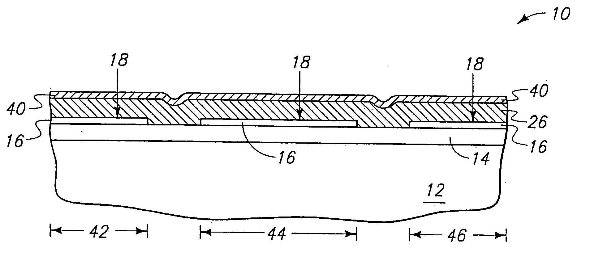
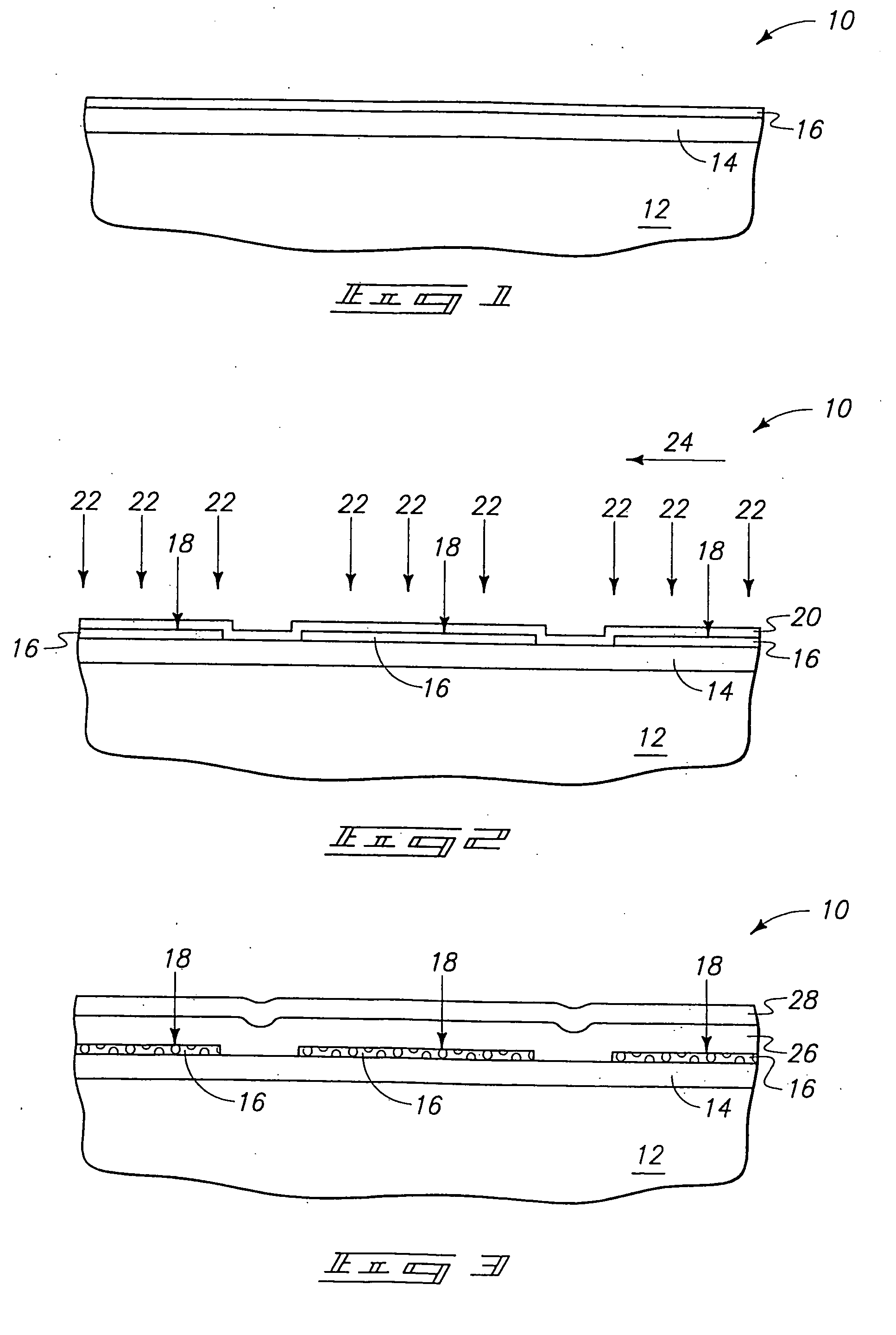
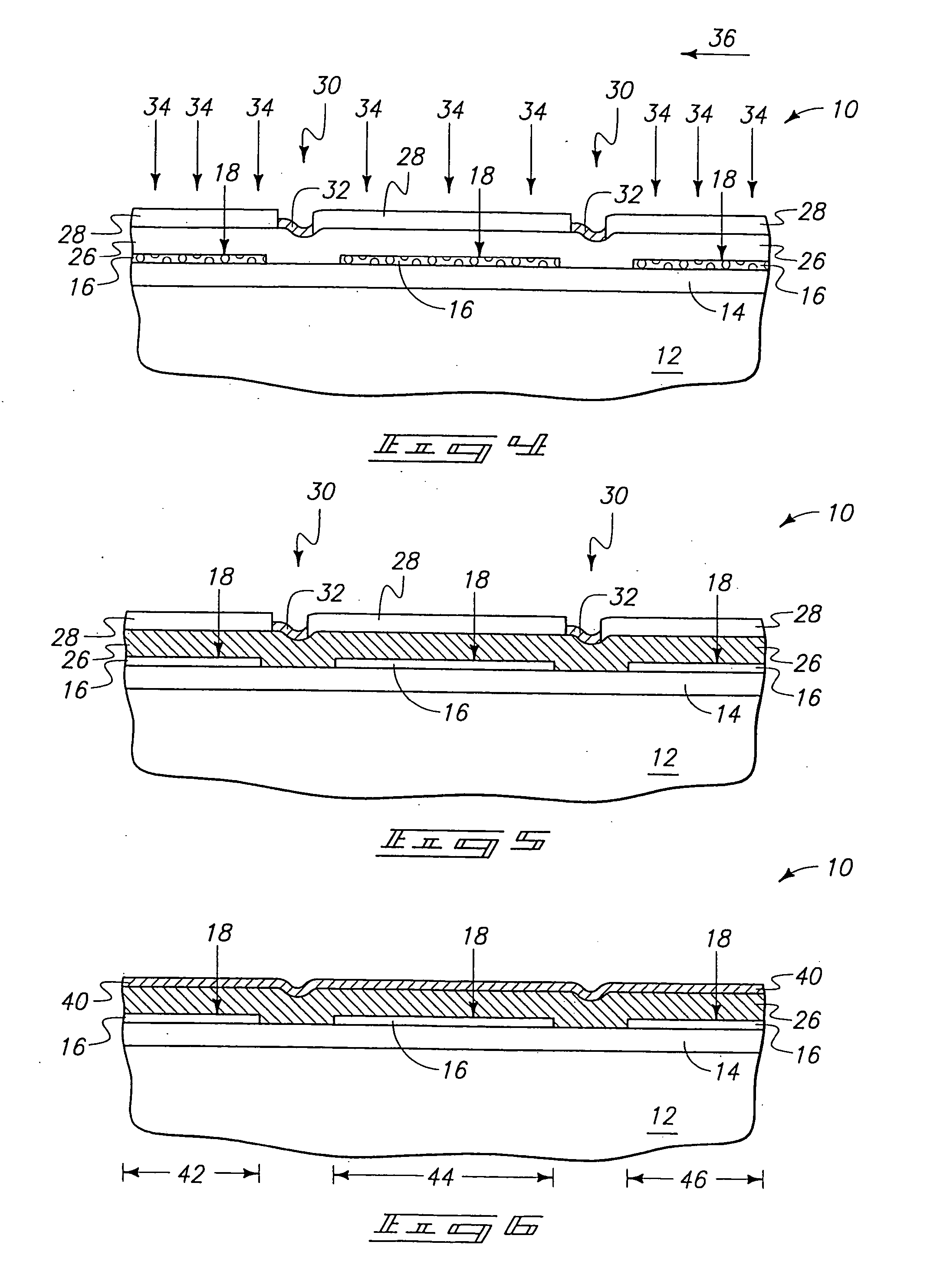
[0038] The invention pertains to logic devices. Exemplary logic devices are described with reference to FIGS. 10-17. Prior to the discussion of the exemplary logic devices, a processing sequence for forming and utilizing preferred TFT-based Si / Ge materials and device structures is described with reference to FIGS. 1-9.

[0039] Referring to FIG. 1, a fragment of a semiconductor construction 10 is illustrated at a preliminary processing stage. To aid in interpretation of the claims that follow, the terms “semiconductive substrate” and “semiconductor substrate” are defined to mean any construction comprising semiconductive material, including, but not limited to, bulk semiconductive materials such as a semiconductive wafer (either alone or in assemblies comprising other materials thereon), and semiconductive material layers (either alone or in assemblies comprising other materials). The term “substrate” refers to any supporting structure, including, but not limited to, the semiconductiv...


PUM


Abstract

The invention includes a TFT-based logic circuit construction. Such construction includes a pair of first transistor devices, and a pair of second transistor devices over the first transistor devices. The first transistor devices have first active regions extending into a first semiconductive material, and the second transistor devices have second active regions extending into a second semiconductive material. At least one of the first and second semiconductive materials can comprise crystalline Si / Ge. The logic construction can comprise NOR circuitry and / or NAND circuitry, as well as higher level logic cells, such as latches. Further, the logic circuit construction can be associated with a semiconductor-on-insulator structure, and on versatile substrates. The invention includes three-dimensional logic cell layout configurations for enhanced wireability and logic cell density, which can lead to enhanced performance.

Description

RELATED PATENT DATA [0001] This patent resulted from a continuation application of U.S. patent application Ser. No. 11 / 130,742, which was filed May 17, 2005, and which is hereby incorporated by reference; which resulted from a continuation application of U.S. patent application Ser. No. 10 / 387,090, which was filed Mar. 11, 2003, issued as U.S. Pat. No. 6,900,667, and is hereby incorporated by reference.TECHNICAL FIELD [0002] This disclosure relates generally to integrated circuits. In particular aspects, the invention pertains to logic devices. The logic devices can be utilized in electronic systems; and can be incorporated into, for example, processor devices for computer systems. BACKGROUND OF THE INVENTION [0003] SOI technology differs from traditional bulk semiconductor technologies in that the active semiconductor material of SOI technologies is typically much thinner than that utilized in bulk technologies. The active semiconductor material of SOI technologies will typically b...

Claims


Application Information

Patent Timeline
Patent Type & Authority Applications(United States)
IPC IPC(8): H01L31/109H01L29/06H01L31/0328H01L31/0336H01L31/072H01L21/822H01L27/06H01L27/12H01L29/10H01L29/786H03K19/096
CPCH01L21/8221H01L21/84H01L27/0688H01L27/10814H01L27/10873H01L27/11807H01L27/1203H01L2924/0002H01L29/1054H01L29/78687H03K19/0963H01L2924/00H10B12/315H10B12/05
Inventor BHATTACHARYYA, ARUP
Owner MICRON TECH INC
Why Eureka
Try Eureka