
Liquid-crystal display device

a liquid crystal display and display device technology, applied in the field of liquid crystal display devices, can solve the problems of disturbing the control of light, affecting and the device is likely to be seen white, so as to reduce the processing accuracy of the casing, suppress the degradation of display quality due to mechanical strain of the lcd panel, and reduce the effect of the flatness of the casing

Inactive Publication Date: 2006-07-20
NEC LCD TECH CORP
View PDF4 Cites 59 Cited by
  • Summary
  • Abstract
  • Description
  • Claims
  • Application Information

AI Technical Summary

Benefits of technology

[0014] A main object of the present invention is to provide an LCD device that suppresses the display quality degradation due to the mechanical strain of the LCD panel, the optical leakage through the gap between the frame-like portion of the casing (i.e., the shield front) and the panel, and the dust penetrated through the gap.
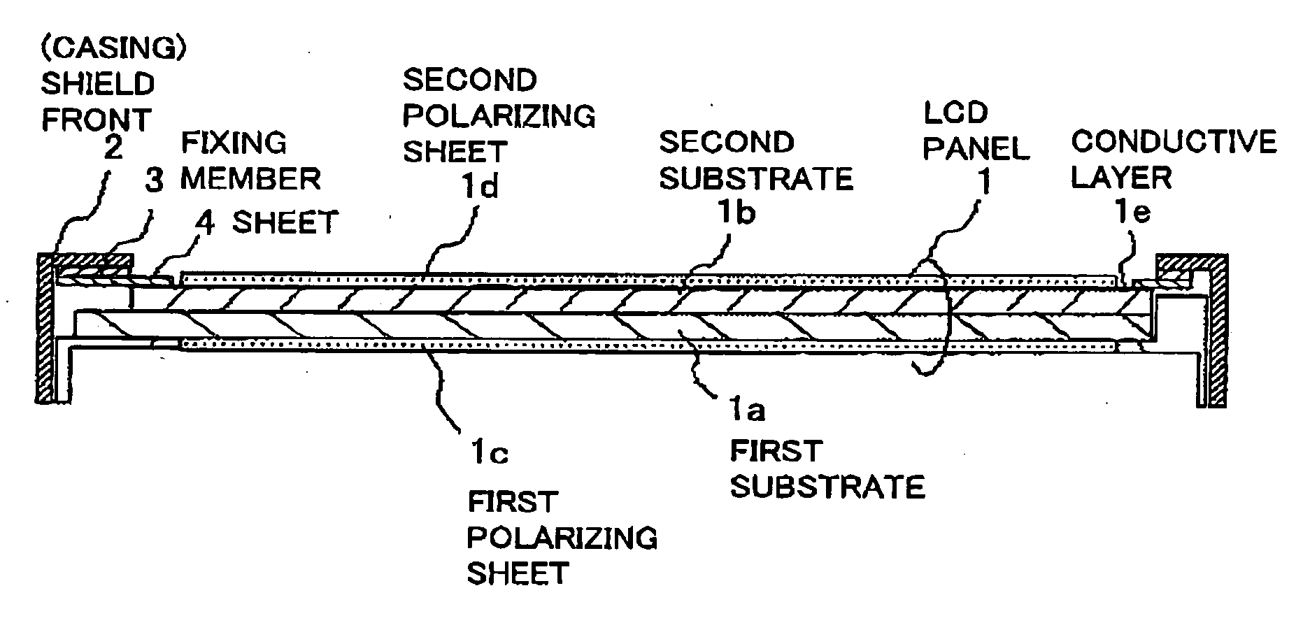
[0017] With the LCD device according to the first aspect of the present invention, the window of the casing is formed to be larger than an outer dimension of the second substrate and therefore, the casing will not contact directly the second substrate even if the processing accuracy of the flatness of the casing is lowered. Only the sheet having electrical conductivity and a light-blocking property is connected to an inner surface of the frame-like portion of the casing and to the layer at the outer portion of the second substrate or on the member. Therefore, strain to be caused in the LCD panel is restrained to a sufficiently low level and at the same time, the orientation disorder of the molecules of the liquid-crystal composite is restrained in a permissible range. Accordingly, the display quality degradation due to the mechanical strain of the LCD panel can be suppressed.
[0018] Moreover, a sheet having electrical conductivity and a light-blocking property is placed in an approximately entire region sandwiched by an outer portion of the second substrate and a frame-like portion of the casing that surrounds the window. An electrically conductive layer is formed directly on or indirectly by way of an optical member on a surface of the second substrate, the surface being located on a side of the window. The sheet is connected to an inner surface of the frame-like portion of the casing and to the layer at the outer portion of the second substrate or on the member. Therefore, electric charges induced by electrification of the surface of the panel are released to the casing by way of the sheet, leakage light generated by diffused reflection in the periphery of the panel is surely blocked, and dust is surely prevented from entering the inside of the casing through the gap between the casing and the panel.

Problems solved by technology

However, the IPS-type LCD device has a disadvantage that the screen of the device is likely to be seen white due to unwanted penetration of light induced by mechanical distortion or deformation of the LCD panel.
The reason of this disadvantage is that mechanical distortion or deformation of the panel causes unwanted change of the orientation of the liquid-crystal molecules and therefore, the control of light is disturbed and unwanted penetration of light will occur.
In this case, the orientation of the liquid-crystal molecules is distorted and the control of light is disturbed and therefore, unwanted penetration of light will occur.
As a result, the screen of the device is likely to be seen white.
However, the weight of a large-sized LCD device of 15-inch or greater exceeds 1 kg and the dimension thereof is considerably large.
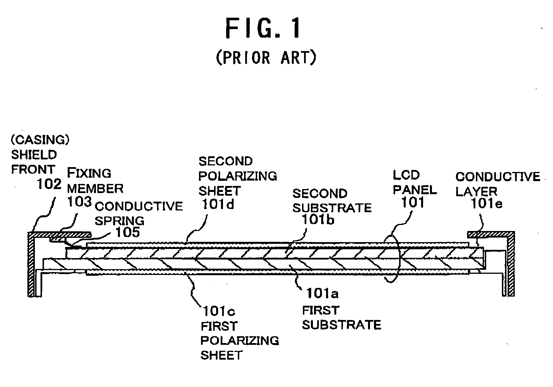
In this case, however, the elongation of the material used is not uniform in the light-shielding portion and the corner portions of the front 102 and therefore, strain is generated in the material.
This means that there arises a disadvantage of an increased thickness of the LCD device.
As a result, the rigidity of the front 102 is reduced to an extremely low value and thus, there arises a disadvantage that torsion deformation is likely to occur in the vicinities of the respective corners of the front 102.
If the gap between the light-shielding portion of the front 102 and the panel 101 is too large, there is a disadvantage that the LCD device is too thick.
To avoid the excessive increase of the said gap by decreasing the said torsion deformation, there is a disadvantage that an amending or adjusting process needs to be carried out after the bending process.
However, if the gap between the picture-frame area of the front 102 and the panel 101 is too large, the thickness of the LCD device will be too large.
Therefore, the picture-frame area of the front 102 will necessitate high processing accuracy of the flatness and as a result, there arises a problem that the processing cost of the front 102 is increased.
As a result, there arises problems that the display quality is lowered by the optical leakage by way of the gap, that display malfunction occurs due to the shade of dust penetrated through the gap, and / or that electrical short-circuit in inner circuitry is induced by conductive dust penetrated through the gap.

Method used


Image

  • Liquid-crystal display device
  • Liquid-crystal display device
  • Liquid-crystal display device

Examples


first embodiment

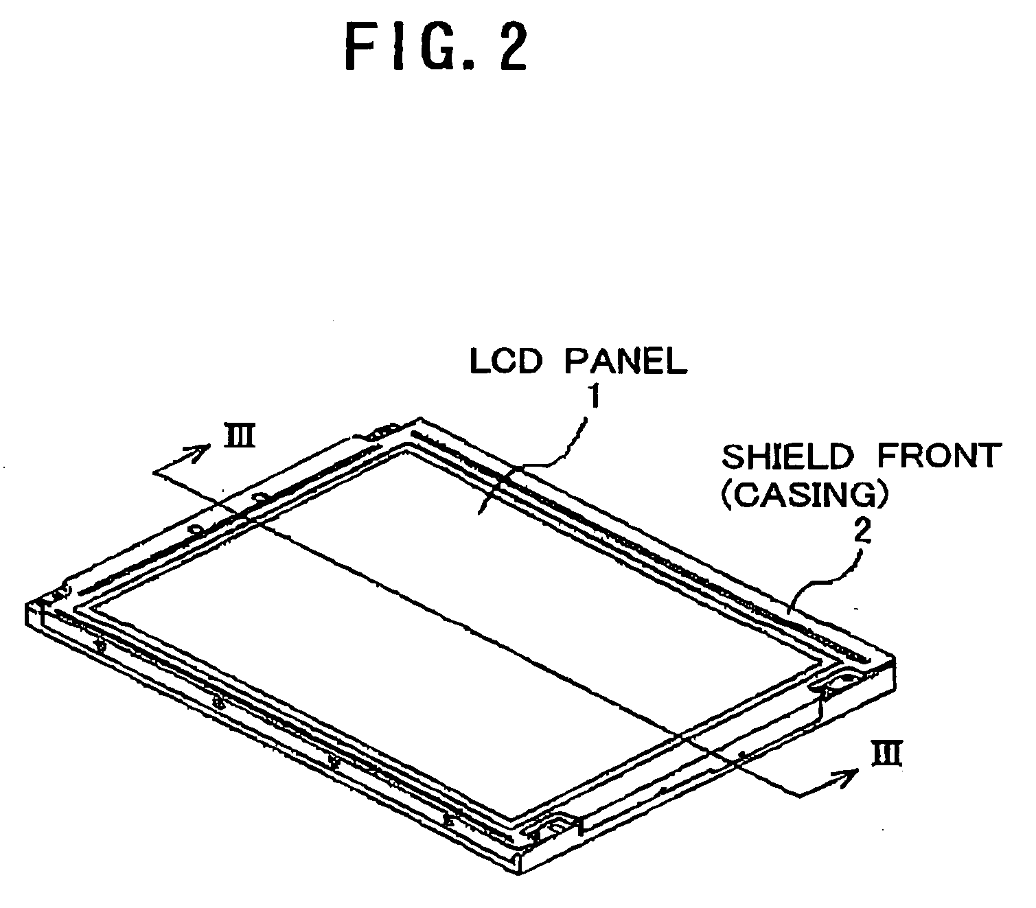
[0050] An LCD device according to a first embodiment of the invention will be explained with reference to FIGS. 2 to 4. FIG. 2 shows the whole structure of the device, FIG. 3 shows the detailed structure thereof, and FIGS. 4A to 4C and FIGS. 8A and 8B show variations of a sheet having electrical conductivity and a light-blocking property used in this device.

[0051] As shown in FIG. 2, the LCD device according to the first embodiment comprises as its main components an LCD panel 1, a backlight unit (not shown) for generating backlight illuminating the panel 1, and a casing or shield front 2 for receiving the panel 1. As shown in FIG. 3, the panel 1 comprises a first transparent substrate 1a, a second transparent substrate 1b, optical members fixed on the surface of the first substrate 1a, and optical members fixed on the surface of the second substrate 1b. An electrically conductive layer 1e, which is made of Indium Tin Oxide (ITO) or the like, is formed on the surface of the second ...

second embodiment

[0072] Next, an LCD device according to a second embodiment of the invention will be explained with reference to FIG. 5.

[0073] With the LCD device according to the above-described first embodiment, the shield front or casing 2 and the sheet 4 are electrically connected to each other with the conductive fixing member 3, as shown in FIG. 3. However, this structure may be modified as shown in FIG. 5.

[0074] In FIG. 5, the sheet 4 is fixed to the inner surface of the frame-like portion of the front 2 with the fixing member 3, like the first embodiment. However, unlike this, the outer end portion of the sheet 4 is bent toward the front 2, thereby directly contacting the sheet 4 with the front 2. In this case, electrical conductivity is not required for the member 3 and therefore, the selection range of material for the member 3 is expanded. As a result, there is an additional advantage that the fixing strength of the member 3 is increased and the usable temperature range is improved.

third embodiment

[0075]FIG. 6 shows an LCD device according to a third embodiment of the invention.

[0076] With the LCD device according to the above-described first embodiment, the sheet 4 is flat, as shown in FIG. 3. However, the shape of the sheet 4 may be modified as shown in FIG. 6.

[0077] Since the window of the front 2 is greater than the outer dimension of the second substrate 1b, there is no possibility that the front 2 contacts the panel 1, even if the distance between the front 2 and the panel 1 is reduced. Therefore, in this embodiment, the sheet 4 has a cross-section with two bends to form a stepwise structure, as shown in FIG. 6. When the LCD device is placed in such a way that the window of the front 2 is located at a top position, a first part of the sheet 4 on the frame-like portion of the front 2 is lower than a second part of the sheet 4 on the outer portion of the second substrate 1b. The inner surface of the frame-like portion of the front 2 is approximately equal to or lower th...


PUM


Abstract

An LCD device suppresses the display quality degradation due to the mechanical strain of an LCD panel, the optical leakage through the gap between the frame-like portion of the casing (the shield front) and the panel, and the dust penetrated through the gap. The window of the casing or shield front is formed to be larger than an outer dimension of the second substrate. A sheet having electrical conductivity and a light-blocking property is placed in an approximately entire region sandwiched by an outer portion of the second substrate and a frame-like portion of the casing that surrounds the window. An electrically conductive layer is formed directly on or indirectly by way of an optical member on a surface of the second substrate, the surface being located on a side of the window. The sheet is connected to an inner surface of the frame-like portion of the casing and to the layer at the outer portion of the second substrate or on the member.

Description

BACKGROUND OF THE INVENTION [0001] 1. Field of the Invention [0002] The present invention relates to a Liquid-Crystal Display (LCD) device. The invention is applicable to any other device or apparatus than the LCD device if it has a structure that components or members are received or enclosed in a frame-shaped casing, for example, a display device employing an organic EL (ElectroLuminescence) element. [0003] 2. Description of the Related Art [0004] There have been strong demands on weight reduction, thinning, and picture-frame-narrowing for the LCD device. To meet such the demands, the use of material and / or structure having higher rigidity has been examined in structural design. The casing for receiving the LCD panel, which is usually called the “shield front”, is one of the structural members of the LCD device. The casing has various functions of increasing the rigidity of the LCD device; protecting the LCD panel, the tape carrier package (TCP) mounted near the panel, and the ele...

Claims


Application Information

Patent Timeline
IPC IPC(8): G02F1/1333
CPCG02F1/133308G02F1/133512G02F2001/133311G02F2001/13332G02F2001/133331G02F2001/133334G02F1/133311G02F1/13332G02F1/133331G02F1/133334G03G15/751G03G2215/00493
Inventor HASEGAWA, FUMIO
Owner NEC LCD TECH CORP
Learn More